Prospects for the development of electronics. Modern problems of electronics. Ways out of this situation
This is my second year teaching the discipline: “Electronics and microprocessor technology.” We discuss industry problems with students in class. In contrast to the topics studied: physical processes in semiconductors, properties p-n junction and transistor characteristics, the problem of domestic microelectronics is well understood by young people. The guys proudly watch videos showing the operation of the S-400 Triumph anti-aircraft missile system, which is controlled by domestic microelectronic developments. The radar system is controlled using central processor“Elbrus” and the result of hitting a target completely depend on a microcircuit measuring 3 by 4 cm. This contributes to the development of interest in the subject.
Today, import substitution in the field of microelectronics affects national security. It seems to me that the country’s leadership, which argued in the 90s that its own electronics were not needed, that they could be purchased abroad, understood perfectly well what they were talking about. It was in this area that the first blow of the shock reforms fell. The electronics industry was one of the first to be destroyed. If in the Soviet Union from 1965 to 1991 there was a Ministry of Electronic Industry of the USSR, for which many research institutes and design bureaus worked, and the development of electronics was decided at the state level, today we hear only pathetic talk about innovation. The work of Soviet scientists and engineers at the turn of 1965-1985 made it possible to bring the USSR to the advanced world level in this field. The system of industrial educational institutions trained personnel for the industry, which no one needed in the 90s.
As an education worker, I find it very difficult to restore the system of industrial education in the field of electronics. When taking the Electronics exam, many young people do not answer the question about the structure of the atom, although they are required to know the operation of electronic devices. This restoration must begin, first of all, with a change in state policy in the field of education. At the turn of the 90s and 2000s, almost all higher and secondary educational institutions were removed from line ministries. The laws of the market dictate completely different relationships between enterprises and educational organizations. As a result, the budgets of universities and colleges were depleted, and many departments closed or were idle, producing not designers, but managers or salespeople.
I believe that it is necessary to identify areas of the country’s life in which not market, but completely different laws should apply: education, healthcare, culture, etc. Then return the system of sectoral educational organizations to the relevant ministries. Within certain industries, the lack of strategic certainty is acutely felt. Increasing efficiency as such, which is read in many of these supposed development strategies, cannot be the goal. Revive and educational organizations, and the industry can precisely achieve strategic certainty. A clearly formulated goal will help formulate requirements for the graduate. And here it is very important to avoid dehumanization vocational education, because today economic feasibility tends to exclude all basic subjects as not profitable, leaving applied skills. The development of professional qualities and spirituality of a specialist must be connected.
“If we take as one unit the level of knowledge at which our students will be in the year they receive a profession, then throughout their working life each of them will have to add another five or six units to their spiritual wealth - otherwise they will lag behind life and will not be able to work successfully.” .
In this article we will talk about the problem modern society electronics engineers. Description of the problem, conclusions and ways out of this situation.
Science cannot be formed without the participation of people who are passionate about it.
Only if you have time, effort and complete immersion these
people in their favorite business can turn out great.
Figure 1. What good intentions lead to.
In this article I would like to describe one of the problems associated with electronics - the problem of the modern electronics community and describe a number of ways out that I see from this situation.
How did I come up with the idea to make this article?
The fact is that for quite a long time I have been conducting a video blog on my YouTube channel. One day I was really boiling and I recorded this video, in which, having prepared myself, I described freelancing in electronics
Then, having received huge feedback from subscribers, I made a second video about the problems faced by electronics engineers and people associated with the production of something new in Russia. In it, in my opinion, I examined in sufficient detail the main problems that I and my colleagues faced.
Now I’m boiling over again, and this is not described in the above material. Therefore, I decided to record a video and write an article. Repetition in written material is necessary because it affects different age audiences of modern engineers. For the generation that is now 18-26 years old (I’m from there), it’s easier to learn about new information by listening, while drawing or doing something. It is much easier for older people to read an article and glean information from it. The school audience, as a rule, does not visit my website/channel on YouTube and so on, since they are simply doing slightly different things.
Description of the essence of the problem being described.
I would like to highlight the problem: the community of domestic electronics engineers itself. We, like any society, have a somewhat specific highly professional language in which we communicate with each other (fetas, juices, stones, etc.), we consist of a large mass of people with similar interests, so I believe that we can distinguish the electronics community in Russia. The problem lies not in interpersonal relationships, but in the systematic problems that people in a given community face.
The first of them is well described by my recent example: A colleague slipped a counterfeit footprint Micro- USB connector and, which led to a number of my difficulties in project work. The chronology of events is approximately as follows:
1. I was going to make a major modification to one of my projects on HF measuring equipment. My colleague and good friend, who is actively promoting this topic, has long asked me to make a convenient and familiar Micro-USB connector on the board for charging a wearable device. I started looking for suitable ready-made footprints and my old friend Mr. X shared his footprint, with a link that he had done this and had everything already debugged.
2. Before using this footprint, I asked Mr. X again if he had used this footprint. To this he replied that yes, and I myself found pictures with confirmation in his album on the social network. I quickly added it to my project and sent the boards to production with full confidence.

Figure 2. Photo of the finished board from production
3. As it turned out, it had a technically impossible feature and the production of PP ( printed circuit boards) returned it to me, pointing out an obvious mistake. This is due to the fact that they cannot make a tricky metalized cut with a diameter ratio of less than 2 to 1. Well, I was not at a loss and quickly corrected it. After that, I wrote to the author, to which I received a rather strange answer: “the footprint is not mine, someone else made it, check it yourself, I have nothing to do with it.” And then he was right. I realized that I did not approach the information received critically and because of this I made a mistake.

Figure 3. Photo from production
4. As it turned out, standard connector It didn’t fit into the resulting footprint, but with the help of a “hammer and persistence” the connector was installed into the resulting footprint. It should be noted that I found a suitable USB connector only in Mitino. In other stores there were others that did not give me a feeling of reliability and footprints of which I still don’t have.
 Figure 4. Photo of the connector itself.
5. This story received an unexpected continuation after the device was fully assembled and debugged. I discovered that all the pins in the connector were swapped. This led to the death of two ltc4054 and the loss of my authority as a developer in the eyes of my colleague. Apparently, the person assigned the numbers based on the first image on Google, which indicated the CONNECTOR FOR THE CABLE. As a result, I had to show considerable skill in wielding a knife in order to carefully cut off part of the polygon on the board and solder it with wires (it looks disgusting) to the ltc4054. I’m ashamed to show a photo of this case, so I won’t put it on the site.
If you abstract from me specifically.
The problem posed is not an isolated instance of manifestation. As soon as I wrote about this in my VK group (at 1 a.m.), a number of comments appeared in the group, and I received several similar situations in messages that people found themselves in. Possible reasons in this I see 4:
1. Complete irresponsibility for your work. The fact is that many young and not very engineers, even in large companies, do work that does not go further than the drawer under the table, which is cleaned daily by the cleaners. In such projects, it makes no difference whether the project can be done or not, whether it works or not, and so on. Such projects are usually carried out by employees in the first six months to a year of their work, so that management and those around them get used to each other.
2. Intentional sabotage on the part of Mr. X. I still don’t know what it could be connected with. But people are different, and maybe the person didn’t like my character or something else? - Maybe. I can't say for sure. But in in a general sense this thing is not correct from my point of view: “If I don’t like someone, I simply don’t help him, or I help at his request, if it’s not difficult for me.”
3. Systematic errors in devices that no one fixes. It happens. During interviews, I saw a bunch of companies that right from the entrance showed how significant they are and how they made 40-50 of their unique devices (that’s a lot) from different areas equipment, most of which simply did not start or had very large jambs. Maybe Mr. X does just that and nothing else. Again, I don't know.
4. This is more student work Mr. X. When you are at a university, no one really cares about such small details.
(if you have your own options for why such things happen, I gladly ask you to write to me and I will add your opinion when mutual understanding is achieved)
Conclusions that I drew from this material:
1) Now in my life I will never use someone else’s footprints, until I receive either factory confirmation of the correct execution of the footprint (touch with my hands and view this piece of the project in electronic form in detail), or before checking it in my debugging using LUT.
2) I will not follow the customer’s lead and push into serial device something untested. As shown this device(photo below), it turns out perfect if you use run-in components and work out the small moments in detail.

Figure 5. Photo of the device in the case
3) Now I will evaluate the quality of the engineers around me, who are so eager to communicate with me, not by the level of their projects, but by such small details. In fact, it may just turn out that a Java/C programmer working for an electronics manufacturing company in his free time traces boards to students and pours all the bullshit on forums on DC-DC converters, although in practice he has never assembled his converters (well or clearly realized why there are different pies like here: link to L5973). If you are a Java/C programmer and most of the time you do Java/C and everything else is a residual, then I see it as fantastic cool topic for discussing Java/C, but in the hardware topic I will require direct real-life data.
4) You should never panic about deadlines. It leads to a large number errors and problems.
Ways out of this situation.
1. Introduction of personal responsibility for one’s work. I personally am always responsible for all the mistakes in my devices. Even if I use someone else's parts.
2. You need to clearly do what you love. If this is your favorite thing, then you will understand it. If not, then don't even try.
Actual problems modern electronics and nanoelectronics Discipline for master's training in the direction
Lesson 1 () Introduction Characteristics professional activity master's degree in the field of preparation Structure and content of the discipline

Scope of discipline and types academic work Semester: 11 Discipline: Current problems of modern electronics and nanoelectronics Direction of training: (2 people) Total labor intensity of the discipline in credit units (ZE) - 4 Lectures: - 9 hours Practical classes: - 36 hours Laboratory exercises: - Extracurricular CRS: - 63 hours Type of certification: exam

Introduction Characteristics of the master’s professional activity in the field of training “Radio Engineering”

OOP in the direction of Graduate in the field of training “Radio Engineering” with the qualification (degree) “Master” in accordance with the tasks of professional activity and the goals of the main educational program must have the following general cultural competencies (GC): the ability to independently learn new research methods, to change the scientific and scientific-production profile of their professional activities (GC-2); ability to use in practice skills and abilities in organizing research and design work, in team management (OK-4);

OOP in the field (continued) The graduate must also have the following professional competencies (PC): general professional: the ability to understand the main problems in their subject area, choose methods and means of solving them (PC 3); By type of activity: design and engineering activities: the ability to analyze the state of a scientific and technical problem by selecting, studying and analyzing literary and patent sources (PC 7);

PLO in the direction (continued) research activities: readiness to compile reviews and reports on the results of ongoing research, prepare scientific publications and applications for inventions, develop recommendations for the practical use of the results obtained (PC 20); organizational and managerial activities: the ability to develop plans and programs for innovative activities in the department (PC 25).

Internet sites 1. – website of the Federal State Institution GNII ITT "Informika"; – federal Internet portal “Nanotechnologies and nanomaterials”; – website “Regulatory documents”; – website “Metrology. Metrological support of production"; – website of the nanotechnology community; 6. www. quality21.ru – website “Quality XXI century”; www. quality21.ru 7. – website of the company “National Instruments”; – website of the journal of the Siberian Federal University website of the journal “Nano- and Microsystem Technology” website of the Institute for Problems of Microelectronics Technology and Highly Pure Materials of the Russian Academy of Sciences

Standards GOST RV GOST RV System for developing and putting products into production. Military equipment. Quality management systems. General requirements GOST RV System for developing and putting products into production. Military equipment. Stages life cycle products and materials GOST RV 0015–101–2010 System for the development and production of products. Military equipment. Tactical and technical (technical) assignment for the implementation of scientific research work GOST RV -2001 System for the development and launch of products into production. Military equipment. The procedure for carrying out scientific research works and their components. Basic provisions……
GOST RV standard
GOST RV
GOST RV SRPP VT. Quality management systems. General requirements ROSSTANDART (Order 6th dated) adopted the state military standard of the Russian Federation GOST RV to replace GOST RV (valid from).

GOST RV standard

Standard ISO 9001:2008 Quality Management Systems. Requirements 7.3 Design and development Planning for design and development The organization shall plan and manage the design and development processes. During design and development planning, the organization shall establish: a) the stages of design and development; b) carrying out analysis, verification and validation appropriate to each stage of design and development; c) design and development responsibilities and authority.

CONSUMER REQUIREMENTS Continuous improvement of the QMS QMS model based on the process approach Measurement, analysis, improvement 7. Life cycle processes Responsibility of management CONSUMER SATISFACTION (4.2,4.9,4.10) (4.3) (4.4) (4.6) (4.7,4.8,4.9,4.10, 4.12 ,4.15,4.19) (4.13) (4.2) (4.2,4.5) (4.2) (4.5) (4.16) (4.1) (4.1,4.18) (4.1,4.9) (4.9) (4.1,4.2) (4.3) ( 4.1) (4.1,4.2) (4.1) (4.2) (4.10,4.17,4.20) (4.9,4.10,4.17,4.20) (4.13) (4.14,4.20) (4.1,4.14) Products OutputInput Value-adding activities (cost ) Information flow 6. Resource management 4. QMS ISO 9001:2008 ISO 9001:1994


Standards GOST R (Electromagnetic compatibility of technical equipment) GOST R Technical means radio communications. Part 1. General technical requirements and test methods GOST R Technical means of radio communication. Part 2. Particular requirements for equipment of paging communication systems GOST R Technical means of radio communication. Part 3. Particular requirements for short-range devices operating at frequencies from 9 kHz to 40 GHz ...... GOST R Technical means of radio communication. Part 6. Particular requirements for digital advanced equipment wireless communication(DECT) GOST R Technical means of radio communication. Part 7. Particular requirements for mobile and portable radio equipment and auxiliary equipment of digital cellular communication systems (GSM and DCS)……


Periodicals (publishing house "Radio Engineering") Magazines: Advances of modern radio electronics; Satellite systems communications and broadcasting; Nanotechnologies: development, application XXI century; Nanomaterials and nanostructures XXI century; Vacuum, plasma and solid state electronics


Automated system ASONIKA for modeling physical processes in radio-electronic means taking into account external influences The monograph presents the works of the Scientific School of Modeling, Information Technologies and Automated Systems (NS MITAS) of Professor A.S. Shalumov and the ASONIKA Scientific School, Professor Yu.N. Kofanov.

Acousto-optical processors of the spectral type Acousto-optical processors of the spectral type are considered, which are a promising class of functional electronics devices that expand the capabilities of modern means signal processing. Original structures of acousto-optical spectrum analyzers with spatial and temporal integration are proposed, planar acousto-optical spectrum analyzers and acousto-optic spectrometers are described.


RFID technology Radio frequency identification technology uses energy electromagnetic field for reading and writing information to a small device - RFID tag. The information on it can be rewritten and supplemented. RFID memory - tags can contain the following information: unique identification number information about the object


Information about the RFID system Based on the reading range, RFID systems can be divided into systems: short-range identification (reading is done at a distance of up to 20 cm); medium-range identification (from 20 cm to 5 m); long-range identification (from 5 m to 100 m) Most RFID tags consist of two parts. First integrated circuit(IC) for storing and processing information, modulating and demodulating radio frequency (RF) signals and some other functions. Second antenna for receiving and transmitting signals.

Methods for recording information on tags The method for recording information depends on design features tags. Depending on this, the following types of tags are distinguished: - RO tags (Read Only) work only to read information. The data required for storage is entered into the tag’s memory by the manufacturer and cannot be changed or deleted during operation. - WORM tags (Write Once Read Many) for writing information once and reading it multiple times. They come from the manufacturer without any user data in the memory device. Necessary information written by the user himself, but only once. If you need to change the data, you will need a new label. - R/W-tags (Read/Write) for multiple recording and multiple reading of information.

Study assignment: Study the requirements of the Federal State Educational Standard and the content of the educational program in the direction of “Radio Engineering” (Master); Study the contents of the article “Nanoelectronics - the basis of information systems of the 21st century”; Get acquainted with the contents of the electronic educational and methodological discipline complex. Note: educational materials posted on the NovSU portal (educational materials > Isaev Vladimir Aleksandrovich > Current problems of modern electronics and nanoelectronics > …) Isaev Vladimir Aleksandrovich > Current problems of modern electronics and nanoelectronics > …)"> 
References 1. Current problems of modern electronics and nanoelectronics: curriculum of the discipline / V. A. Yuzova, G. N. Shelovanova. - Krasnoyarsk: IPK SFU, Current problems of modern electronics and nanoelectronics: a course of lectures / G. N. Shelovanova. - Krasnoyarsk: IPK SFU, Borisenko V.E. Nanoelectronics - the basis of information systems of the XXI century // Soros educational journal, 1997, 5, p. Design and principle of operation of a translucent electron microscope: Electronic educational manual / A.I. Bobrov, A.V. Pirogov, N.O. Krivulin, D.A. Pavlov; edited by D.A. Pavlova. - Nizhny Novgorod: Nizhny Novgorod State University, p.

References (continued) 5. GOST R Technical means of radio communication. Part 6. Particular requirements for digital advanced wireless communication (DECT) equipment 6. GOST R Technical means of radio communication. Part 7. Particular requirements for mobile and portable radio equipment and auxiliary equipment of digital cellular communication systems (GSM and DCS) 7. Automated system ASONIKA for modeling physical processes in radio-electronic equipment taking into account external influences / Ed. A.S. Shalumova. - M: Publishing House "Radio Engineering", - 424 p.

Thank you for your attention! Tel.: (8162)

This publication is part of the electronic educational and methodological complex in the discipline “Current problems of modern electronics and nanoelectronics.” including the discipline curriculum, laboratory workshop, a guide to course work, guidelines for independent work, control and measuring materials “Current problems of modern electronics and nanoelectronics. Bank test tasks", visual aid "Current problems of modern electronics and nanoelectronics. Presentation materials."
This publication presents materials reflecting current state micro- and nanoelectronics, as well as prospects for the development of these industries.
Designed for students in the master's program 210100.68 "Electronics and Microelectronics" of the enlarged group 210000 "Electronics, radio engineering and communications", and can also be used by anyone interested in electronics and nanoelectronics.
Microclusters and their energy state.
In a number of cases, the traditional approach to controlling the properties of semiconductor materials encounters fundamental limitations:
absence in nature of impurities with suitable properties;
low solubility limit of atoms of many impurities in the crystal lattice of a semiconductor;
high concentration of electrically active intrinsic lattice defects in the alloyed material, etc.
In this regard, in last years is actively developing new approach to control the properties of semiconductors, based on the formation of nano-sized clusters in the semiconductor matrix, which may include atoms of introduced impurities, atoms of their own components, as well as their own point defects of the crystal lattice.
Table of contents
PREFACE
LECTURE 1 THE ROLE OF SURFACE IN THE CREATION OF MICRO- AND NANOELECTRONICS DEVICES
1.1. Surface and its properties
1.2. Surface potential
1.3. Surface states. Tamm levels
1.4. Fast and slow surface states
Self-test questions
LECTURE 2 MICRO- AND NANO-SIZED ATOMIC CLUSTERS IN SEMICONDUCTORS AND THEIR PROPERTIES
2.1. Microclusters and their energy state
2.2. Methods for obtaining and applying structures with atomic clusters
2.3. Interphase boundaries and their properties
2.4. Possibility of forming structures with minimal mismatch in lattice parameters
2.5. Strained semiconductor structures, their properties and applications
Self-test questions
LECTURE 3 TECHNOLOGICAL CAPABILITIES OF PROMISING TYPES OF EPITAXY
3.1. Advances in molecular beam epitaxy
3.2. Vapor phase epitaxy from organometallic compounds
Self-test questions
LECTURE 4 CREATION OF INTEGRAL DEVICES BY LITHOGRAPHY METHODS
4.1. Traditional photolithography and its problems
4.2. Electron beam lithography
4.3. X-ray lithography
Self-test questions
LECTURE 5 HIGH RESOLUTION LITHOGRAPHY
5.1. Maskless technology methods
5.2. Electron and ion beam as a tool modern technology
Self-test questions
LECTURE 6 QUANTUM FOUNDATIONS OF NANOENGINEERING
6.1. Quantization effect
6.2. Quantum limitation
6.3. Interference effects
6.4. Tunneling
6.5. Devices based on quantum effects
Self-test questions
LECTURE 7 LOW-DIMENSION SILICON MEDIA
7.1. The relevance of using low-dimensional silicon in the production of micro- and nanoelectronics products
7.2. Formation of low-dimensional silicon
7.3. Structural modifications of porous silicon
7.4. Application of low-dimensional silicon
Self-test questions
LECTURE 8 TECHNOLOGY OF THIN FILMS AND MULTILAYER STRUCTURES
8.1. Introduction
8.2. Mechanisms of epitaxial growth of thin films
8.3. Liquid phase epitaxy
8.4. Vapor phase epitaxy from organometallic compounds
8.5. Molecular beam epitaxy
Self-test questions
LECTURE 9 QUANTUM ENGINEERING
9.1. Introduction
9.2. Dimensional quantization. Quantum dots
9.3. Fabrication of heterostructures with quantum dots
9.4. SCT research methods
9.5. Lasers based on self-organized quantum dots
9.6. Superlattices
Self-test questions
LECTURE 10 MULTILAYER NANOSTRUCTURES
10.1. Multilayer deposition by magnetron sputtering
10.2. Electrolytic deposition
10.3. Surface nanostructures
10.4. Obtaining surface structures using the MBE method
10.5. Obtaining surface structures by gas-phase epitaxy
10.6. Chemical assembly of surface nanostructures
10.7. Low-dimensional structures based on porous silicon
10.8. Carbon nanotubes
Self-test questions
LECTURE 11 PHYSICAL NATURE OF SUPERCONDUCTIVITY
11.1. Concept of superconductivity
11.2. Superconductors of the first and second kind
11.3. Bardeen-Cooper-Schrieffer theory
11.4. Josephson effect
11.5. Meissner effect
Self-test questions
LECTURE 12 HIGH TEMPERATURE SUPERCONDUCTIVITY
12.1. History of the discovery of high-temperature superconductivity
12.2. Methods for obtaining HTSC films
12.3. Application of HTSC materials
Self-test questions
LECTURE 13 MICROWAVES AND THEIR NATURE
13.1. Discovery of the thermal effects of microwaves
13.2. Physical nature of microwaves
13.3. Microwave transmission and communications
13.4. Ultrahigh frequency therapy
Self-test questions
LECTURE 14 ELEMENT BASE OF MICROWAVE SYSTEMS
14.1. History of the laser
14.2. Semiconductor lasers
14.3. Nanolasers
14.4. Light Emitting Diodes
14.5. Fiber optic cables
Self-test questions
LECTURE 15 COMMUNICATION SYSTEMS
15.1. Systems television broadcasting
15.2. Satellite connection
15.3. mobile connection
15.4. cellular
15.5. Optoelectronic systems
Self-test questions
LECTURE 16 TEMPERATURE AND RADIATION RESISTANCE OF ELECTRONIC TECHNOLOGY PRODUCTS NIKI
16.1. Introduction
16.2. Temperature resistance and heat transfer mechanisms
16.3. Heat removal methods
16.4. Promising liquid dielectrics for cooling
16.5. Cryogenic electronics
16.6. The influence of radiation on the parameters of electronic devices
Self-test questions
LECTURE 17 PROSPECTS FOR SILICON AS A MATERIAL FOR EXTREME ELECTRONICS
17.1. Silicon-on-insulator structures and their advantages
17.2. Technologies for manufacturing SOI structures
17.3. KNS structures, their advantages and application prospects
17.4. Advantages and prospects of silicon carbide electronics
Self-test questions
LECTURE 18 MATERIALS AND STRUCTURES OF EXTREME ELECTRONICS
18.1. Silicon carbide - material for extreme electronics
18.2. The possibilities of carbon in solving problems of extreme electronics
18.3. Structures and devices of extreme electronics
Self-test questions
CONCLUSION
BIBLIOGRAPHICAL LIST.
Problems, prospects and import substitution
A discussion of the current situation and prospects of the contract electronics market in Russia took place at the conference “Contract manufacturing of electronics in Russia” as part of the Expoelectronics exhibition, held at Crocus Expo from March 24 to 26.
The seminar was organized by the Russian office of Jabil, and a significant part concerned the discussion of work and organization of production processes within the company. However, a significant part of the conference was devoted to the state of the industry as a whole and the problems facing it. Let's try to dwell on this point in more detail.
Contract manufacturing: Russian features
The main thing for modern contract manufacturing is strict optimization of all costs. To be competitive and efficient in modern market, the manufacturer has to use any available methods saving, literally making sure not a single penny goes to waste. After all, even penny losses, multiplied by large volumes characteristic of contract manufacturing, result in impressive figures. Therefore, you need to be ready to optimize everything: the technologies used, production processes, salaries. Well, your appetite for profit should also be moderated.
According to Semyon Lukachev (director of PC Altonika LLC), in contract manufacturing the price consists of three main components:
- Logistics
- Component cost
- Cost of work
The remaining components, as Semyon Lukachev noted in his answers to questions, are of a secondary nature. It will be possible to think about their optimization when the main issues in three main areas have been resolved.
Interestingly, Sergei Zorin, director of business development at Jabil, also addressed the issue of cost components in his speech.

Here the ratio is slightly different from the approximate estimate of Semyon Lukachev, but the information from Sergei Zorin’s slide covers the production of electronics as a whole, i.e. a noticeably broader process.
The cost of work in the final price of the product is, as a rule, small and amounts to somewhere around 10-15%, but it is still not worth placing contract manufacturing in large cities: due to the high cost of rent, labor and other resources, the total costs will be too high in order to maintain competitiveness. It is better to place contract manufacturing in small towns and regions where rental rates and wages are not too high.
Thus, the most serious impact on contract manufacturing in Russia, i.e. the price of the final product, is exerted by logistics and component costs.
Logistics
Parts and components are mainly delivered from Chinese factories, i.e. they are imported. And in matters of import into the Russian Federation, several “tight spots” arise.
Firstly, in Russia there are companies that have been working on the market since the 90s and have maintained the same work pattern: they carry goods “by weight”. When using gray schemes, the overhead costs for delivering components from China are about 15%, while with white schemes it is about 35%, a significant share of which is VAT. Therefore, a legal supplier can achieve at least approximately comparable prices only subject to relatively large volumes of supplies, which are often unprofitable due to the too small size of the Russian market.
In general, the small volume of the market in many cases acts as an independent negative factor: manufacturers are forced to work with small volumes supplies of components, in which logistics overhead costs are high per unit of production, which negatively affects the cost of the final product and its competitiveness in the market.
Cost of components and difficulties with them
However, even with the selection of parts and components in China, not everything is so simple.
Firstly, the Chinese are very reluctant to share detailed specifications and documentation for equipment and components. Sometimes you have to literally gnaw out documentation with your teeth. Specifications may be incomplete, incorrect, or even incorrect. All this significantly complicates the adaptation process and production, since it is very difficult to understand what works and how.
Secondly, even if there is documentation, you always need to be prepared for the fact that a redesign will be required. The Chinese use a large number of components, for example, controllers, which are available only on the domestic market - they even mark them only in hieroglyphs. Information about such components is almost impossible to find, and without this it is impossible to understand what the same controller does. The parts themselves are difficult to find even on the domestic market, and besides, they are too expensive to transport here due to narrow niche and small volumes.
Thirdly, it is difficult to find the right balance between price and quality of such parts. The Chinese on the domestic market can somehow find the right balance, when the chip is already quite cheap, but still more or less works and has an acceptable defect rate. But only the Chinese who are on the spot can do this. In Russia, you have to choose components with more stable quality, but a higher price.
Other difficulties
But in addition to the objective ones, there are also subjective difficulties associated with the “peculiarities of doing business” in Russia.
Semyon Lukachev noted separately: he himself Russian market doesn't really want to move. Many companies already have a stable pool of customers, thanks to which they ensure a certain profitability, and are not at all eager to get involved in other low-profit projects, where they will have to carefully calculate the risks and squeeze the maximum out of production and personnel. Although there are a few exceptions where managers are ready to fight for the project.
The situation is approximately the same with customers: in principle, they exist and could work with Russian manufacturers on a mutually beneficial basis. But they are used to ordering everything from China, which no longer looks like a “cheap alternative”, and they are also not particularly keen on optimization and increasing efficiency.
However, it is precisely this direction - the reorientation of Russian manufacturers and customers towards each other - that has very great potential. It’s just that to implement it you need to work hard, you need a desire to expand and master new projects, you need passion. But most often this is not the case; everyone wants stable, unhurried work. But only the development of mass serial production will ensure stability and work “on the back”, and will allow us to attract companies currently working with the Chinese who are engaged in final assembly.
Current situation in the contract manufacturing market of electronics in the world
Sergei Zorin, now director of development at Jabil, and recently the owner of his own electronics production in the Moscow region, spoke about global trends.

The total volume of the global electronics market today is approximately 1.3 trillion. dollars, contract production is 35-40%. The main growth driver for the entire segment is consumer electronics, where the main research and production potential is concentrated (in Russia the picture is very different). And from this technology then flows into other related industries.
Two most actively developing areas consumer electronics- wearable electronics and smart home control. In principle, automotive electronics are also developing, but development there is largely hampered by very high safety requirements, since the cost of an error can cost people’s lives. Therefore, safety assessment and verification take a lot of time and effort in this area.
The second trend is that the already established system is gradually being destroyed, in which China was the only and universal production base for the whole world, from where products were distributed throughout the world. different countries. Now production is slowly shifting to the customer and end consumer markets. There is strong price competition.
In general, the main factors of market development look like this:

All manufacturers are divided into four large groups:

For the global electronics industry, the same law applies as for many other industries: “The largest 20% of companies hold 80% of the market, and the remaining 80% of small enterprises hold 20% of the market.” Even a little is violated in favor of large companies.

Large and small manufacturers have their own advantages and disadvantages. It is quite obvious that large companies have higher production efficiency. Here's an approximate ratio:

Finally, it is quite predictable that the main contract manufacturing companies are located in Asia, and the trend towards strengthening this region will continue in the near future.
If we come closer to Russia, it is worth noting that contract manufacturing of electronics in Russia is small even in comparison with other European countries.

As you can see, Russia is in 27th place. To my surprise, Hungary is in first place by a large margin, and Bulgaria is in second.
On the other hand, if we look at production costs, including labor costs, Russia today does not look like an outsider.

If China noticeably wins in terms of labor costs for operators (i.e., relatively unskilled employees), then Russia is much more profitable in terms of the cost of engineering personnel.
State of the electronics contract manufacturing market in Russia
Moving on to the state of the Russian market, let's start with a few numbers. The total volume of the electronics market in Russia is $34 billion. Electronics production is $6 billion (18%), contract manufacturing is $710 million (i.e., only 2% of the total market).
Market in numbers: data and forecasts
The contract manufacturing market is growing in terms of money, but it is interesting to note that the growth of production itself is noticeably lower than the growth of the market as a whole. “Extra” growth is formed due to additional services, configurations, etc. This was discussed in the speech of Ivan Pokrovsky, general director of the information and analytical agency Center for Modern Electronics.

This section also contains slides from his report.

According to the Center for Advanced Electronics, the contract manufacturing market volume is about $250 million (which differs from the above figures due to a different research base). This figure includes production abroad for Russian companies, contract production in Russia for Russian companies, and contract production in Russia for foreign companies.
The market volume and its growth are presented more clearly in the diagram.
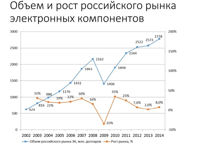
It is interesting that, despite a rather serious failure in 2008-2009, the market quite quickly recovered to its previous level. However, after this, his growth began to rapidly slow down.
Ivan also presented a growth forecast for 2015.

And a chart with the forecast until 2018:

By 2018, the total market volume should be about $382 million, and the growth rate will decrease to 20%. However, you probably shouldn’t pay special attention to growth rates in general: firstly, the high numbers are explained by the recovery after the crisis, and secondly, the base is too low to draw any conclusions. And finally, this is a forecast.
Growth trends. Import substitution factor
The comprehensive chart shows the major growth drivers of the industry.

The industry is growing in many ways not quantitatively, but qualitatively: manufacturers provide comprehensive services, helping customers solve additional problems.

Accordingly, the development of a network of contract manufacturing, united by a unified management system and logistics service, is seen as promising models. Increasing the efficiency of investments in management systems, logistics and marketing. Plus the development of the ODM direction - production of standard products own development under the customer's brand. This makes it possible to quickly realize the potential of import substitution.
How the Russian market works: industries, applicability, penetration
So, let’s now see what the Russian market for contract manufacturing of electronics consists of. For starters, all electronics production in Russia, broken down by industry. Diagram from Sergei Zorin's speech (here we're talking about about everyone production):

And from the speech of Ivan Pokrovsky (here we take into account contractual production):

It's interesting to compare the difference, isn't it?

Sergey Zorin noted important feature Russian market: a significant part of electronics production is limited to the military industry and products for government agencies, while these manufacturers are not present on the open market, and their activities have practically no impact on the industry. This is sad, because in to a large extent hinders the development of the market as a whole.
Russian manufacturers
It's funny, but despite the above considerations, Moscow and St. Petersburg today occupy leading positions in the production of electronics.

However, the situation may change depending on whether companies are counted based on the location of their head office or their actual factories.
And this is what the list of leading manufacturers in Russia looks like, according to the Center for Modern Electronics. By sales volume:

And in terms of production volumes:

Printed circuit board production
He talked about the production of printed circuit boards CEO Rezonit company, Andrey Kucheryavyi. To be honest, this is the main activity of his company, and contract manufacturing is secondary. However, there was a lot in the speech interesting information about the market as a whole.

The volume of which this speaker also assessed as “modest”.

At the same time, the entire printed circuit board market is indicated for Russia; if we take production itself, then this is about 25% of 300 million (i.e., about $80 million), and such a share on the graph will be completely invisible.

In figures, the market volume is somewhere around 12-13 million dm2 per month (production is a quarter of this figure).
On the one hand, the crisis has significantly damaged the Russian market. At the end of 2014, supplies of electronic components increased significantly as companies stocked up. So now we can expect a failure in both supplies and production. On the other hand, the devaluation of the ruble has significantly increased the competitiveness of our enterprises, thanks to which production in Russia now looks more preferable in many situations than even in China. For example, Latvia used to look very good thanks to low level wages, with salaries of 300-400 euros. Now the enterprises there have largely lost their attractiveness. As for the rise in prices within the country, for the company’s plant in Klin (it is engaged in mass production), when the ruble fell by half, the cost increased by about a quarter.
First of all, during a crisis, mass orders fall. This market fell already in September 2014, and in 2014 overall, the volume of orders in China fell by a quarter. In 2015, the decline continued and now the reduction is about another 10%. Thus, the overall market decline today is about a third.
Also, according to the director of Rezonit, from the experience of past crises we can conclude that the workload of contract manufacturing feels the crisis after 4-5 months. At the same time, the segment of orders and production of small-scale prototypes has grown, largely due to the flow of orders from China. After the fall of the ruble, the cost of fulfilling orders at Chinese enterprises has increased significantly, and now Russian enterprises represent an interesting alternative, especially for small-scale production. The fact is that in China they don’t like small orders, because there’s a lot of fuss with them. Therefore, Chinese manufacturing enterprises, as a rule, in addition to basic prices, also charge a one-time fee for “preparation for production,” which in many cases can be quite high. So they cut off small-scale customers in order to focus on larger orders. This feature allows Russian enterprises to occupy a niche in the development, refinement and production of small batches of electronic boards.

The decrease in the value of the ruble greatly changed the balance of forces in the market, so a significant volume of orders began to flow from China to Russia. Moreover, the number of such orders and the total volume are not so small: since the end of last year, production capacities have been well loaded. At some point there was even a danger that Russia would run out of fiberglass. However, mass production, especially for complex orders, is also gradually moving to Russia. Russian enterprises in Lately actively invested in technology, and now many orders that previously went to China or even Japan, because local manufacturers could not fulfill them, remain in Russia.
A moment of new technologies: “In Klin they began to make multilayer boards, hybrid boards, introduced new finishing coatings, and will produce boards with impedance control on own production. By the fall we will switch to new technological standards, there will be 100 microns in all layers and an area of 0.2-0.4. We are learning a lot of new technologies. Next year we will launch flexible and flexible-rigid ones, reduce the thickness and increase the number of layers to 20, etc.”
By the way, here too the speaker noted that too small a market volume hinders the development of the industry. For example, although significant investments are often made in new technologies and equipment, as a result this equipment and technology remains unclaimed because they can only be used effectively for large production volumes, and such a volume of orders simply does not exist. For example, to operate a new machine you need to pour 500 liters of solder and keep it heated, which is pointless given the current state of the market.
State. Help or harm?
Assessments were divided on this issue, but they were all in the “red zone”. The state does not need electronics production - in best case scenario. The market is weak, it is not yet able to promote itself, and officials do not want to do this. As a result, there is now a generally stupid situation on the market: large retailers have lobbied for a reduction in import customs duties on electronics, and duties on electronic components stayed with the old one, high level. This is such discrimination against a domestic manufacturer who simply doesn’t give a damn. Help came from unexpected places: the actively criticized entry into the WTO. Thanks to the import duty reduction plan, duties on electronic components should be reduced or eliminated from September 2015, after which the industry could become more profitable.

In Russia there is also no second growth driver for any market - government orders. More precisely, it exists, and it is very significant. But, as industry representatives say, this area is largely closed in on itself: enterprises tied to government orders produce something for the state, have good profitability for themselves and absolutely do not want to risk money on the open market.


