Signal integrity on the printed circuit board and characteristic impedance of the conductors. PCB layout
December 11, 2016 at 5:48 pmLittle secrets of tracing boards with operational and instrument amplifiers
- Internet of Things,
- Sound ,
- Electronics for Beginners
- Tutorial
When designing boards
Nothing comes so cheap
And not valued so highly
How to properly trace.

In the age of the Internet of things and the availability of printed circuit boards, and not only using LUT technology, their design is often carried out by people whose entire activity is related to digital technology.
Even when tracing is simple digital board There are unspoken rules that I always follow in my projects, and in the case of developing measuring devices with digital-analog circuit sections, this is simply necessary.
In this article, I want to direct novice designers to a number of elementary techniques that should be followed in order to obtain a stable operating circuit and reduce the measurement error or minimize the distortion coefficient of the audio path. For clarity, the information is presented in the form of two examples.
Example number two. Tracing a simple op-amp circuit

Rice. 1. Op-amp amplifier circuit

Rice. 2. Two options for tracing the amplifier board to the op-amp
A small off-topic, not directly related to the topic of today’s article
I strongly advise you to use the same technique when supplying power to other types of microcircuits, especially ADCs, DACs and numerous power pins of microcontrollers. If you use built-in analog microcontroller modules - ADC, DAC, comparators, reference voltage sources, do not be lazy to look at the datasheet and see which blocking capacitors, in what quantity, and where should be installed. An decoupling circuit in the form of a filter or at least a resistance between the main digital power supply of the microcontroller and the analog one would not hurt. It is better to place the analog ground as a separate polygon or screen layer, and connect it to the main ground at one point, in some cases it is useful through a filter
Circuit elements feedback should be located as close as possible to the non-inverting input, which minimizes the possibility of interference with the high-impedance input circuit.
Let's move on to a more serious and interesting case from the field of measurements, where tracing can be extremely important.
Example number one. Tracing a current consumption monitor on an instrumentation amplifier

Rice. 3. Current monitor circuit using instrumentation op-amp
The figure shows a diagram of a current consumption meter. The measuring element is the shunt resistance included in the power circuit. The load at which the current is measured is R load. The measured voltage is removed from the resistance R shunt and filtered using a symmetrical circuit on elements R1, R2, C1-C3. Chip U2 serves to supply the reference voltage. R4, C5 - output filter.
When tracing, of course, you must follow all the recommendations given above.

Rice. 4. Two options for routing the amplifier board on an instrumentation op-amp
Let's look at the shortcomings that the left diagram has:
- Since we have a differential input, it is necessary to make its two signal paths as symmetrical as possible. The signal line conductors must be of the same length and located close to each other. Ideally at the same distance from each other;
- The reference follower IC must be located as close as possible to the reference voltage input of the instrumentation amplifier.
Do not keep a loaded gun on the wall. One day it will definitely shoot and choose the most inconvenient moment for this.
As noted just above, the circuits are different: digital part; analog part; power section; interface part. All these parts of the chain must be spatialized if possible. Otherwise, “miracles” may happen. So, for example, if your device has a touchpad (the capacitance is drawn by the copper substrate on the board), and next to it you place pulse converter power source, then interference will lead to false alarms. Another example: placing a power part, such as a relay, near the digital or analog part can, in the worst case, damage the internals of the microcontroller, creating a potential higher than 5 volts on the pin, and give false positives (in the digital part) or incorrect readings (in the analog part), however, if the ADC resolution does not exceed 10 bits, then the grounds do not need to be separated, since the impact is usually minimal).
By making the lands “different”, you reduce the impact they have on each other. What should you follow when cultivating land?
By maximizing the ground area of the PCB, its inductance is minimized, which in turn leads to reduced radiation. Plus, by increasing the area, the noise immunity of the printed circuit board increases. There are two ways to increase the area: completely fill the board or make it in the form of a grid.
Full filling allows you to get the lowest impedance - this is an “ideal” earth system (the mesh is a little worse).
However, on large-area boards, continuous filling with an earthen polygon can. The polygon should be placed on both sides of the board as evenly as possible. Using the grid, you need to control its step: .
Polygons on multilayer boards must be connected in several places; below is a “Faraday cage” in the design of a printed circuit board. This technique is used at gigahertz frequencies.

If the ground is routed as a simple trace, then it is recommended to route the power line on the opposite side of the board. In the case of a multilayer board, the ground and power lines are also located on different layers.
The resistance of the conductors also depends on the frequency (see. ). The higher the frequency, the higher the trace/ground resistance. So, for example, if at 100 Hz the ground resistance is 574 μOhm, and the signal track (width 1 mm, length 10 mm, thickness 35 μm) is 5.74 mOhm, then at a frequency of 1 Hz they will take values of 11.6 mOhm and 43 .7 Ohm. As you can see, the difference is colossal. In addition, the board itself begins to emit radiation, especially in the areas where the wires are connected to the board.
We looked at the “ground” from a general point of view, but going into specifics, we need to discuss the so-called “signal” ground, where:
A) single-point connection is an undesirable topology from a noise point of view. Because of serial connection ground impedance increases, which leads to problems on high frequencies. The acceptable range for this topology is from 1 Hz to 10 MHz, provided that the longest ground trace does not exceed 1/20 of the wavelength.

B) a multipoint connection has a significantly lower impedance - recommended in digital circuits and at high frequencies. Connections should be as short as possible to minimize resistance. In circuits with low frequencies, this topology is not the best choice. If the board has a LF and HF part, then the HF should be placed closer to ground, and the LF closer to the power line.

C) hybrid connection - it is recommended to use it if there are different components on one printed circuit board: digital part, analog or power. They operate at different frequencies and should not be mixed for greater accuracy and stability of the device.

Example of land division:

In our case (roughly speaking) there is only one part - digital. There will be connectors on the board, but the currents passing through them are insignificant (programmer, UART pin for Wi-Fi module) and should not affect the operation of the device. Despite the fact that the clock frequency of the microcontroller is 24 MHz, all peripherals with which it is connected will operate at frequencies significantly less than 10 MHz (with the exception of the Wi-Fi module, which has a frequency of 2.4 GHz). In other words, our device can use a single-point connection, but a multi-point system is also suitable. It is also recommended to place the polygon under all non-emitting high-frequency circuits (like our microcontroller, but we'll talk about that later).

When using a full fill for a landfill, it is worth removing the copper under the Wi-Fi module - this will avoid shielding its radiation.

All isolated copper sections (eng. dead copper) must be removed, because at RF they begin to radiate and interfere with signal lines. The potential in such areas is different from the ground and is undesirable.

In addition to the ground/polygon, there are other tracks on the board - signal tracks. They can carry a clock signal (for example, the SCK line of the MAX7219 chip) or transmit data (UART RX and TX tracks from the Wi-Fi module). Wiring them is no less responsible - you need to know a few rules. Firstly, to minimize interference from one conductor to another, the distance between them should be maintained.
For clock signals, as well as audio, video and reset lines, it is recommended to leave at least two trace widths on the sides. In particularly critical cases, they try to avoid intersecting tracks on the opposite side of the board.
Surely you have already seen printed circuit boards of various devices - and noticed that most of them do not have right angles.
At high frequencies they will act as antennas, so when turning they resort to angles of 45 degrees.
Previously, printed circuit boards were drawn by hand, which means the angles were arbitrary (not strictly 45 degrees). From an EMC point of view, this layout is better, but does not allow the board to be presented in a more understandable form. At the moment, all modern CAD systems predominantly support .

Among other things, when turning 90 degrees, which means in powerful chains with high currents this can lead to overheating and burning out of the area. In low-frequency circuits, the use of T-shaped connections is not prohibited, but in high-frequency circuits this will lead to problems.
On the other hand, sharp corners should be avoided - this is bad from a technological point of view. In such places, a “stagnation” of chemical reagents forms, and during etching, part of the conductor will simply be etched away.

Among other things, the width of the conductor must be constant, because when it changes, the track begins to behave like an antenna. Via holes are not recommended to be placed on the pad or in close proximity to the element (without separating them with a solder mask), since this can lead to solder flow and, as a result, cause defects during assembly. It is best to cover the vias with a solder mask.

Elements that are connected to the landfill must be separated by a thermal barrier, which helps prevent uneven heating of the site during soldering.

Microcontroller
We've covered the basics of PCB layout, now it's time to move on to specific things, in particular, consider the best practices for routing the power and ground lines of the microcontroller.

Blocking capacitors must be placed as close as possible to the microcontroller terminals so that they are located along the “path” of the current. Otherwise there is simply no point in them.

For single-sided printing, the template looks like this:

In the case of a double-sided board, it is convenient to place the capacitors under the microcontroller, but with a large batch and automatic installation this will cause technical difficulties. Usually they try to place the components on one side.

Quartz resonator, the clock source, should also be located as close to the legs as possible. Single sided board:

All jumpers between the legs of SMD chips must be located outside the soldering area:

And finally, some useful tips.

GENERAL CONSIDERATIONS
Due to the significant differences between analog and digital circuitry, the analog portion of the circuit must be separated from the rest, and special methods and rules must be followed when wiring it. Effects arising from non-ideal characteristics of printed circuit boards become especially noticeable in high-frequency analog circuits, but errors general view, described in this article, may affect the quality characteristics of devices operating even in the audio frequency range.
The intent of this article is to discuss common mistakes made by PCB designers, describe the impact of these mistakes on quality performance, and provide recommendations for resolving problems that arise.
Printed circuit board - circuit component
Only in rare cases can an analog circuit PCB be routed so that the influences it introduces do not have any effect on the operation of the circuit. At the same time, any such impact can be minimized so that the characteristics of the analog circuitry of the device are the same as those of the model and prototype.
Layout
Developers digital circuits can correct small errors on the manufactured board by adding jumpers to it or, conversely, removing unnecessary conductors, making changes to the operation of programmable microcircuits, etc., moving very quickly to the next development. This is not the case for an analog circuit. Some of the common errors discussed in this article cannot be corrected by adding jumpers or removing excess conductors. They can and will render the entire printed circuit board inoperative.
It is very important for a digital circuit designer using such correction methods to read and understand the material presented in this article well in advance of submitting the design to production. A little design attention and discussion of possible options will not only prevent the PCB from becoming scrap, but also reduce the cost of gross errors in a small analog part of the circuit. Finding errors and fixing them can result in hundreds of lost hours. Prototyping can reduce this time to one day or less. Breadboard all your analog circuits.
Sources of noise and interference
Noise and interference are the main elements that limit the quality of circuits. Interference can be either emitted by sources or induced on circuit elements. Analog circuitry is often located on a printed circuit board along with high-speed digital components, including digital signal processors ( DSP).
High frequency logic signals generate significant RF interference ( RFI). The number of sources of noise emission is enormous: key power supplies for digital systems, mobile phones, radio and television, lamp power supplies daylight, personal computers, lightning discharges, etc. Even if an analog circuit operates in the audio frequency range, radio frequency interference can create noticeable noise in the output signal.
The choice of PCB design is important factor, which determines the mechanical characteristics when using the device as a whole. Materials used to make printed circuit boards various levels quality. It will be most suitable and convenient for the developer if the printed circuit board manufacturer is located nearby. In this case, it is easy to control the resistivity and dielectric constant - the main parameters of the printed circuit board material. Unfortunately, this is not enough and knowledge of other parameters such as flammability, high-temperature stability and hygroscopicity coefficient is often necessary. These parameters can only be known by the manufacturer of the components used in the production of printed circuit boards.
Layered materials are designated by the indices FR ( flame resistant, resistance to ignition) and G. Material with index FR-1 has the highest flammability, and FR-5 - the least. Materials with indexes G10 and G11 have special characteristics. Printed circuit board materials are given in table. 1.
Do not use FR-1 category PCB. There are many examples of FR-1 PCBs that have suffered thermal damage from high-power components. Printed circuit boards in this category are more similar to cardboard.
FR-4 is often used in the manufacture of industrial equipment, while FR-2 is used in the manufacture of household appliances. These two categories are standardized in the industry, and FR-2 and FR-4 PCBs are often suitable for most applications. But sometimes the imperfect characteristics of these categories force the use of other materials. For example, for very high-frequency applications, fluoroplastic and even ceramics are used as printed circuit board materials. However, the more exotic the PCB material, the higher the price may be.
When choosing a PCB material, pay special attention to its hygroscopicity, since this parameter can have a strong negative effect on the desired characteristics of the board - surface resistance, leakage, high-voltage insulating properties (breakdown and sparking) and mechanical strength. Also pay attention to operating temperature. Plots with high temperature may occur in unexpected places, such as near large digital integrated circuits that switch at high frequencies. If such areas are located directly below analog components, increased temperatures may affect the performance of the analog circuit.
Table 1
|
Components, comments |
|
|
paper, phenolic composition: pressing and stamping at room temperature, high hygroscopicity coefficient |
|
|
paper, phenolic composition: applicable for single-sided printed circuit boards of household appliances, low hygroscopicity coefficient |
|
|
paper, epoxy composition: designs with good mechanical and electrical characteristics |
|
|
fiberglass, epoxy composition: excellent mechanical and electrical properties |
|
|
fiberglass, epoxy composition: high strength at elevated temperatures, non-flammable |
|
|
fiberglass, epoxy composition: high insulating properties, highest strength of fiberglass, low hygroscopicity coefficient |
|
|
fiberglass, epoxy composition: high flexural strength at elevated temperatures, high solvent resistance |
Once the PCB material is selected, the thickness of the PCB foil needs to be determined. This parameter is primarily selected based on the maximum value of the flowing current. If possible, try to avoid using very thin foil.
NUMBER OF PRINTED BOARD LAYERS
Depending on the overall circuit complexity and quality requirements, the designer must determine the number of layers of the PCB.
Single Layer PCBs
Very simple electronic circuits are made on single-sided boards using cheap foil materials (FR-1 or FR-2) and often have many jumpers, resembling double-sided boards. This method of creating printed circuit boards is recommended only for low frequency circuits. For reasons that will be described below, single-sided printed circuit boards are highly susceptible to interference . A good single-sided PCB is quite difficult to design for many reasons. Nevertheless, there are good boards of this type, but when designing them, you need to think a lot in advance.
Double Layer PCBs
On next level There are double-sided printed circuit boards, which in most cases use FR-4 as the substrate material, although FR-2 is also sometimes found. The use of FR-4 is more preferable, since the holes in printed circuit boards made from this material are of better quality. Circuits on double-sided printed circuit boards are much easier to wire because In two layers it is easier to route intersecting routes. However, for analog circuits, crossing traces is not recommended. Where possible, the bottom layer ( bottom) must be allocated under the landfill, and the remaining signals must be routed in the upper layer ( top). Using a landfill as an earth bus provides several advantages:
- the common wire is the most frequently connected wire in the circuit; therefore, it is reasonable to have “a lot” of common wire to simplify wiring.
- the mechanical strength of the board increases.
- the resistance of all connections to the common wire decreases, which, in turn, reduces noise and interference.
- The distributed capacitance for each circuit circuit is increased, helping to suppress radiated noise.
- the polygon, which is a screen, suppresses interference emitted by sources located on the side of the polygon.
Double-sided PCBs, despite all their advantages, are not the best, especially for low-signal or high-speed circuits. In general, the thickness of the printed circuit board, i.e. the distance between the metallization layers is 1.5 mm, which is too much to fully realize some of the advantages of a two-layer printed circuit board given above. The distributed capacity, for example, is too small due to such a large interval.
Multilayer PCBs
For critical circuit design, multilayer printed circuit boards (MPBs) are required. Some reasons for their use are obvious:
- The distribution of power buses is just as convenient as for the common wire bus; if polygons on a separate layer are used as power buses, then it is quite simple to supply power to each circuit element using vias;
- signal layers are freed from power buses, which facilitates the wiring of signal conductors;
- Distributed capacitance appears between the ground and power polygons, which reduces high-frequency noise.
In addition to these reasons for using multilayer printed circuit boards, there are other, less obvious ones:
- better electromagnetic suppression ( EMI) and radio frequency ( RFI) interference due to the reflection effect ( image plane effect), known back in the time of Marconi. When a conductor is placed close to a flat conducting surface, most of the high frequency return currents will flow along the plane directly below the conductor. The direction of these currents will be opposite to the direction of the currents in the conductor. Thus, the reflection of the conductor in the plane creates a signal transmission line. Since the currents in the conductor and in the plane are equal in magnitude and opposite in direction, some reduction in radiated interference is created. The reflection effect only works effectively with unbroken solid polygons (these can be both ground polygons and power polygons). Any loss of integrity will result in reduced interference suppression.
- reduction in overall cost for small-scale production. Although multilayer PCBs are more expensive to manufacture, their potential radiation is lower than that of single- and double-layer PCBs. Therefore, in some cases, using only multilayer boards will allow you to meet the emission requirements set during design, without additional testing and testing. The use of MPP can reduce the level of radiated interference by 20 dB compared to double-layer boards.
Layer order
Inexperienced designers often have some confusion about the optimal order of PCB layers. Let's take for example a 4-layer chamber containing two signal layers and two polygon layers - a ground layer and a power layer. What is the best layer order? Signal layers between polygons that will serve as screens? Or should we make the polygon layers internal to reduce the interference of signal layers?
When addressing this issue, it is important to remember that often the location of the layers does not matter much, since the components are located on the outer layers anyway, and the buses that supply signals to their pins sometimes pass through all the layers. Therefore, any screen effects are just a compromise. In this case, it is better to take care of creating a large distributed capacity between the power and ground polygons, placing them in the inner layers.
Another advantage of placing the signal layers outside is the availability of signals for testing, as well as the possibility of modifying connections. Anyone who has ever changed the connections of conductors located in the inner layers will appreciate this opportunity.
For PCBs with more than four layers, there is general rule place high-speed signal conductors between the ground and power polygons, and route low-frequency signal conductors to the outer layers.
GROUNDING
Good grounding - general requirement rich, multi-level system. And it should be planned from the first step of design development.
Basic rule: division of land .
Dividing the earth into analog and digital parts is one of the simplest and most effective methods noise suppression. One or more layers of a multilayer printed circuit board are usually dedicated to a layer of ground polygons. If the developer is not very experienced or inattentive, then the ground of the analog part will be directly connected to these polygons, i.e. analog current return will use the same circuit as digital return current. Auto-distributors work in much the same way and unite all the lands together.
If a previously developed printed circuit board with a single ground polygon combining analog and digital grounds is subject to processing, then it is necessary to first physically separate the grounds on the board (after this operation, the operation of the board becomes almost impossible). After this, all connections are made to the analog ground of the analog circuit components (analog ground is formed) and to the digital ground of the digital circuit components (digital ground is formed). And only after this, digital and analog ground are combined at the source.
Other rules for land formation:

Almost all clock signals are high enough frequency signals that even small capacitances between traces and polygons can create significant couplings. It must be remembered that it is not only the fundamental clock frequency that can cause a problem, but also its higher harmonics.
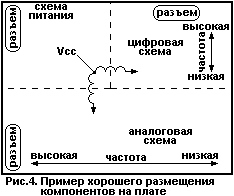
Example of good component placement
Figure 4 shows a possible layout of all components on the board, including the power supply. This uses three separate and isolated ground/power planes: one for the source, one for the digital circuit, and one for the analog circuit. The ground and power circuits of the analog and digital parts are combined only in the power supply. High-frequency noise is filtered out in the power circuits by chokes. In this example, the high frequency signals of the analog and digital parts are separated from each other. This design has a very high probability of a favorable outcome, since it is ensured good accommodation components and following the rules of circuit separation.
There is only one case where it is necessary to combine analog and digital signals over an analog ground area. Analog-to-digital and digital-to-analog converters placed in housings with analog and digital ground pins. Taking into account the previous discussion, it can be assumed that the digital ground pin and analog ground pin should be connected to the digital and analog ground buses, respectively. However, in this case this is not true.
The names of the pins (analog or digital) refer only to the internal structure of the converter, to its internal connections. In the circuit, these pins must be connected to the analog ground bus. The connection can also be made internally integrated circuit, however, it is quite difficult to obtain a low resistance of such a connection due to topological restrictions. Therefore, when using converters it is assumed outer join analog and digital ground pins. If this is not done, then the parameters of the microcircuit will be significantly worse than those given in the specification.
It must be taken into account that the digital elements of the converter can degrade the quality characteristics of the circuit by introducing digital noise into the analog ground and analog power circuits. This is taken into account when developing converters. negative impact so that the digital part consumes as little power as possible. At the same time, interference from switching logic elements is reduced. If the digital pins of the converter are not heavily loaded, then internal switching usually does not cause special problems. When designing a PCB containing an ADC or DAC, careful consideration must be given to decoupling the converter's digital power supply to analog ground.
FREQUENCY CHARACTERISTICS OF PASSIVE COMPONENTS
For proper operation analog circuits are very important right choice passive components. Start your design by carefully considering the high-frequency characteristics of passive components and preliminary placement and layout of them on the board sketch.
A large number of designers completely ignore the frequency limitations of passive components when used in analog circuitry. These components have limited frequency ranges and operating them outside the specified frequency range can lead to unpredictable results. Some may think that this discussion only concerns high-speed analog circuits. However, this is far from true - high-frequency signals have a strong impact on the passive components of low-frequency circuits through radiation or direct communication through conductors. For example, a simple low-pass filter on an op-amp can easily become a high-pass filter when exposed to high frequency at its input.
Resistors
The high frequency characteristics of resistors can be represented equivalent circuit shown in Figure 5.
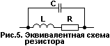
There are three types of resistors commonly used: 1) wirewound, 2) carbon composite, and 3) film. It doesn't take much imagination to understand how a wirewound resistor can be converted into an inductance, since it is a coil of wire made of high-resistance metal. Most developers electronic devices have no idea about the internal structure of film resistors, which are also a coil, albeit made of a metal film. Therefore, film resistors also have an inductance that is less than that of wirewound resistors. Film resistors with a resistance of no more than 2 kOhm can be freely used in high-frequency circuits. The resistor terminals are parallel to each other, so there is a noticeable capacitive coupling between them. For high-value resistors, the terminal-to-terminal capacitance will reduce the total impedance at high frequencies.
Capacitors
The high-frequency characteristics of capacitors can be represented by the equivalent circuit shown in Figure 6.
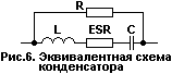
Capacitors in analog circuits are used as decoupling and filtering components. For an ideal capacitor, the reactance is determined by the following formula:
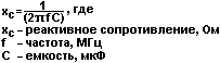
Therefore, a 10 µF electrolytic capacitor will have a resistance of 1.6 ohms at 10 kHz and 160 µohms at 100 MHz. Is it so?
When using electrolytic capacitors, care must be taken correct connection. The positive terminal must be connected to a more positive constant potential. Incorrect connection leads to DC flow through the electrolytic capacitor, which can damage not only the capacitor itself, but also part of the circuit.
In rare cases, the DC potential difference between two points in the circuit may change its sign. This requires the use of non-polar electrolytic capacitors, the internal structure of which is equivalent to two polar capacitors, connected in series.
Inductance
The high-frequency characteristics of inductances can be represented by the equivalent circuit shown in Figure 7.

Inductance reactance is described by the following formula:
![]()
Therefore, a 10 mH inductance will have a reactance of 628 ohms at 10 kHz, and a reactance of 6.28 megohms at 100 MHz. Right?
Printed circuit board
The printed circuit board itself has the characteristics of the passive components discussed above, although not so obvious.
The pattern of conductors on a printed circuit board can be both a source and a receiver of interference. Good wiring reduces the sensitivity of the analog circuit to radiation sources.
The printed circuit board is susceptible to radiation because the conductors and leads of the components form a kind of antenna. Antenna theory is a rather complex subject to study and is not covered in this article. However, some basics are provided here.
A bit of antenna theory
On DC or low frequencies the active component predominates. As the frequency increases, the reactive component becomes more and more significant. In the range from 1 kHz to 10 kHz, the inductive component begins to take effect and the conductor is no longer a low-impedance connector, but rather acts as an inductor.
The formula for calculating the inductance of a PCB conductor is as follows:

Typically, traces on a printed circuit board have values from 6 nH to 12 nH per centimeter of length. For example, a 10 cm conductor has a resistance of 57 mOhm and an inductance of 8 nH per cm. At a frequency of 100 kHz, the reactance becomes 50 mOhm, and at higher frequencies the conductor will be an inductance rather than a resistive one.
The rule for a whip antenna is that it begins to noticeably interact with the field at about 1/20 of the wavelength, and maximum interaction occurs at a rod length of 1/4 of the wavelength. Therefore, the 10 cm conductor from the example in the previous paragraph will start to become a pretty good antenna at frequencies above 150 MHz. It must be remembered that although the generator clock frequency A digital circuit may not operate at frequencies above 150 MHz; its signal always contains higher harmonics. If the printed circuit board contains components with pin pins of considerable length, then such pins can also serve as antennas.
The other main type of antenna is loop antenna. The inductance of a straight conductor increases greatly when it bends and becomes part of an arc. Increasing inductance lowers the frequency at which the antenna begins to interact with the field lines.
Experienced PCB designers with a reasonable understanding of loop antenna theory know not to design loops for critical signals. Some designers, however, do not think about this, and the return and signal current conductors in their circuits are loops. The creation of loop antennas is easy to demonstrate with an example (Fig. 8). In addition, the creation of a slot antenna is shown here.

Let's consider three cases:
Option A is an example of bad design. It does not use an analog ground polygon at all. The loop circuit is formed by the ground and signal conductors. When a current passes, an electric field and a magnetic field perpendicular to it arise. These fields form the basis loop antenna. The loop antenna rule states that for best efficiency, the length of each conductor should be equal to half the wavelength of the received radiation. However, we should not forget that even at 1/20 of the wavelength, the loop antenna is still quite effective.
Option B better option A, but there is a gap in the polygon, probably to create a specific place for routing signal conductors. The signal and return current paths form a slot antenna. Other loops form in the cutouts around the chips.
Option B - example best design. The signal and return current paths coincide, negating the effectiveness of the loop antenna. Note that this design also has cutouts around the chips, but they are separated from the return current path.
The theory of signal reflection and matching is close to the theory of antennas.
When the PCB conductor is rotated through an angle of 90°, signal reflection may occur. This is mainly due to changes in the width of the current path. At the apex of the corner, the trace width increases by 1.414 times, which leads to a mismatch in the characteristics of the transmission line, especially the distributed capacitance and the trace's own inductance. Quite often it is necessary to rotate a trace on a printed circuit board by 90°. Many modern CAD packages allow you to smooth the corners of drawn routes or draw routes in the form of an arc. Figure 9 shows two steps to improve the corner shape. Only the last example maintains a constant path width and minimizes reflections.

Tip for experienced PCB designers: leave the smoothing process for the last stage of work before creating teardrop-shaped pins and filling polygons. Otherwise, the CAD package will take longer to smooth due to more complex calculations.
Capacitive coupling occurs between PCB conductors on different layers when they intersect. Sometimes this can create a problem. Conductors placed one above the other on adjacent layers create a long film capacitor. The capacity of such a capacitor is calculated using the formula shown in Figure 10.

For example, a printed circuit board may have the following parameters:
- 4 layers; the signal and ground polygon layers are adjacent,
- interlayer spacing - 0.2 mm,
- conductor width - 0.75 mm,
- conductor length - 7.5 mm.
The typical ER dielectric constant for FR-4 is 4.5.
Substituting all the values into the formula, we get a capacitance value between these two buses equal to 1.1 pF. Even such a seemingly small capacity is unacceptable for some applications. Figure 11 illustrates the effect of a 1 pF capacitance when connected to the inverting input of a high-frequency op-amp.

It can be seen that the amplitude of the output signal doubles at frequencies close to the upper limit of the frequency range of the op-amp. This, in turn, can lead to oscillation, especially at antenna operating frequencies (above 180 MHz).
This effect gives rise to numerous problems, for which there are, however, many ways to solve them. The most obvious of them is reducing the length of the conductors. Another way is to reduce their width. There is no reason to use a conductor of this width to connect the signal to the inverting input, because Very little current flows through this conductor. Reducing the length of the trace to 2.5 mm and the width to 0.2 mm will lead to a decrease in capacitance to 0.1 pF, and such capacitance will no longer lead to such a significant increase in the frequency response. Another solution is to remove part of the polygon under the inverting input and the conductor that goes to it.
The width of the PCB conductors cannot be reduced indefinitely. The limit width is defined as technological process, and the thickness of the foil. If two conductors pass close to each other, then a capacitive and inductive coupling is formed between them (Fig. 12).
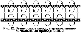
Signal conductors should not be routed parallel to each other, except in the case of differential or microstrip lines. The gap between conductors should be at least three times the width of the conductors.
Capacitance between traces in analog circuits can create problems with large resistor values (several megohms). The relatively large capacitive coupling between the inverting and non-inverting inputs of an op-amp can easily cause the circuit to oscillate.

For example, with d=0.4 mm and h=1.5 mm (fairly common values), the inductance of the hole is 1.1 nH.
Remember that if there are large resistances in the circuit, then special attention should be paid to cleaning the board. During the final operations of manufacturing a printed circuit board, any remaining flux and contaminants must be removed. Recently, when installing printed circuit boards, water-soluble fluxes are often used. Being less harmful, they are easily removed with water. But at the same time, washing the board with insufficiently clean water can lead to additional contamination that worsens the dielectric characteristics. Therefore, it is very important to clean the high-impedance circuit board with fresh distilled water.
SIGNAL ISOLATION
As already noted, interference can penetrate into the analog part of the circuit through the power supply circuits. To reduce such interference, decoupling (blocking) capacitors are used to reduce the local impedance of the power buses.
If you need to lay out a printed circuit board that has both analog and digital parts, then you need to have at least a small understanding of electrical characteristics logical elements.
A typical output stage of a logic element contains two transistors connected in series with each other, as well as between the power and ground circuits (Fig. 14).

These transistors ideally operate strictly in antiphase, i.e. when one of them is open, then at the same moment in time the second is closed, generating either a logical one or a logical zero signal at the output. In the steady state logic state, the power consumption of the logic element is small.
The situation changes dramatically when the output stage switches from one logic state to another. In this case, for a short period of time, both transistors can be open simultaneously, and the supply current of the output stage increases greatly, since the resistance of the current path from the power bus to the ground bus through two series-connected transistors decreases. Power consumption increases abruptly and then also decreases, which leads to local change supply voltage and the occurrence of a sharp, short-term change in current. These changes in current result in the emission of radio frequency energy. Even on a relatively simple printed circuit board there may be tens or hundreds of considered output stages of logic elements, so the total effect of their simultaneous operation can be very large.
It is impossible to accurately predict the frequency range in which these current surges will occur, since the frequency of their occurrence depends on many factors, including the propagation delay of switching transistors of the logic element. The delay, in turn, also depends on many random reasons that arise during the production process. Switching noise has a broadband distribution of harmonic components over the entire range. There are several methods for suppressing digital noise, the application of which depends on the spectral distribution of the noise.
Table 2 shows the maximum operating frequencies for common capacitor types.
table 2
From the table it is obvious that tantalum electrolytic capacitors are used for frequencies below 1 MHz; at higher frequencies, ceramic capacitors should be used. It must be remembered that capacitors have their own resonance and their incorrect choice may not only not help, but also aggravate the problem. Figure 15 shows typical self-resonances of two common capacitors - 10 μF tantalum electrolytic and 0.01 μF ceramic.
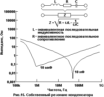
Actual specifications may vary between different manufacturers and even from batch to batch within the same manufacturer. It is important to understand that for efficient work capacitor, the frequencies it suppresses must be in a lower range than the frequency of its own resonance. Otherwise, the nature of the reactance will be inductive, and the capacitor will no longer work effectively.
Do not be mistaken that one 0.1 µF capacitor will suppress all frequencies. Small capacitors (10 nF or less) can operate more efficiently at higher frequencies.
IC power decoupling
Decoupling the power supply of integrated circuits to suppress high-frequency noise consists of using one or more capacitors connected between the power and ground pins. It is important that the conductors connecting the leads to the capacitors are short. If this is not the case, then the self-inductance of the conductors will play a significant role and negate the benefits of using decoupling capacitors.
A decoupling capacitor must be connected to each chip package, regardless of whether there are 1, 2, or 4 op-amps inside the package. If the op amp is dual-supplied, then it goes without saying that decoupling capacitors should be located at each power pin. The capacitance value must be carefully selected depending on the type of noise and interference present in the circuit.
In particularly difficult cases, it may be necessary to add an inductance connected in series with the power output. The inductance should be located before, not after, the capacitors.
Another, cheaper way is to replace the inductance with a resistor with low resistance (10...100 Ohms). In this case, together with the decoupling capacitor, the resistor forms a low-pass filter. This method reduces the power supply range of the op-amp, which also becomes more dependent on power consumption.
Typically, to suppress low-frequency noise in power circuits, it is sufficient to use one or more aluminum or tantalum electrolytic capacitors at the power input connector. An additional ceramic capacitor will suppress high-frequency interference from other boards.
ISOLATION OF INPUT AND OUTPUT SIGNALS
Many noise problems result from directly connecting input and output pins. As a result of the high-frequency limitations of passive components, the response of a circuit when exposed to high-frequency noise can be quite unpredictable.
In a situation where the frequency range of induced noise is to a large extent differs from the frequency range of the circuit, the solution is simple and obvious - placing a passive RC filter to suppress high-frequency interference. However, when using a passive filter, you must be careful: its characteristics (due to the non-ideal frequency characteristics of passive components) lose their properties at frequencies 100...1000 times higher than the cutoff frequency (f 3db). When using series-connected filters tuned to different frequency ranges, the higher frequency filter should be closest to the source of interference. Ferrite ring inductors can also be used to suppress noise; they retain the inductive nature of resistance up to a certain certain frequency, and above their resistance becomes active.
Tips on analog circuit can be so large that it is only possible to get rid of (or at least reduce) them through the use of screens. To operate effectively, they must be carefully designed so that the frequencies producing biggest problems, could not get into the scheme. This means that the screen should not have holes or cutouts larger than 1/20 of the wavelength of the radiation being screened. Good idea Allocate sufficient space for the proposed shield from the very beginning of PCB design. When using a shield, you can optionally use ferrite rings (or beads) for all connections to the circuit.
OPERATIONAL AMPLIFIER CASES
One, two, or four operational amplifiers are usually placed in one package (Fig. 16).
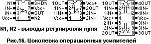
A single op amp often also has additional inputs, for example to adjust the offset voltage. Dual and quad op amps have only inverting and non-inverting inputs and output. Therefore, if it is necessary to have additional adjustments, it is necessary to use single operational amplifiers. When using additional outputs, you must remember that by their structure they are auxiliary inputs, so they must be controlled carefully and in accordance with the manufacturer's recommendations.
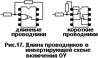
In a single op amp, the output is located on the opposite side of the inputs. This can make it difficult to operate the amplifier at high frequencies due to the long feedback lines. One way to overcome this is to place the amplifier and feedback components on different sides printed circuit board. This, however, results in at least two additional holes and cuts in the ground polygon. Sometimes it is worth using a dual op amp to solve this problem, even if the second amplifier is not used (and its pins must be connected properly). Figure 17 illustrates the reduction in the length of the feedback circuit conductors for an inverting connection.
Dual op amps are especially common in stereo amplifiers, and quad op amps are used in multistage filter circuits. However, there is a rather significant disadvantage to this. Although modern technology provides decent isolation between the signals of amplifiers located on the same silicon chip, there is still some crosstalk between them. If it is necessary to have a very small amount of such interference, then it is necessary to use single operational amplifiers. Crosstalk does not only occur when using dual or quad amplifiers. Their source can be the very close proximity of passive components of different channels.
Dual and quad op-amps, in addition to the above, allow for more dense installation. The individual amplifiers appear to be mirror-image relative to each other (Fig. 18).

Figures 17 and 18 do not show all connections required for normal operation, for example, a mid-level shaper with unipolar power supply. Figure 19 shows a diagram of such a shaper when using a quad amplifier.

The diagram shows all the necessary connections to implement three independent inverting stages. It is necessary to pay attention to the fact that the conductors of the half-supply voltage driver are located directly under the integrated circuit housing, which makes it possible to reduce their length. This example illustrates not what should be, but what should be done. The average level voltage, for example, could be the same for all four amplifiers. Passive components can be sized accordingly. For example, frame size 0402 planar components match the pin spacing of a standard SO package. This allows conductor lengths to be kept very short for high frequency applications.
3D AND SURFACE MOUNTING
When placing op amps in DIP packages and passive components with lead wires, vias must be provided on the printed circuit board to mount them. Such components are currently used when there are no special requirements for the dimensions of the printed circuit board; They are usually cheaper, but the cost of the printed circuit board increases during the manufacturing process due to drilling additional holes for component leads.
In addition, when using external components, the dimensions of the board and the length of the conductors increase, which does not allow the circuit to operate at high frequencies. Vias have their own inductance, which also limits the dynamic characteristics of the circuit. Therefore, overhead components are not recommended for implementing high-frequency circuits or for analog circuits located close to high-speed logic circuits.
Some designers, trying to reduce the length of the conductors, place resistors vertically. At first glance it may seem that this shortens the length of the route. However, this increases the path of current through the resistor, and the resistor itself represents a loop (turn of inductance). The emitting and receiving ability increases many times over.
Surface mounting does not require a hole for each component lead. However, problems arise when testing the circuit, and it is necessary to use vias as test points, especially when using small components.
UNUSED OP-AMP SECTIONS
When using dual and quad op-amps in a circuit, some sections may remain unused and must be connected correctly in this case. Incorrect connections can lead to increased power consumption, more heat, and more noise from the op amps used in the same package. The pins of unused operational amplifiers can be connected as shown in Fig. 20a. Connecting pins with additional components(Fig. 20b) will make it easy to use this op-amp during setup.

CONCLUSION
Remember the following basic points and keep them in mind at all times when designing and wiring analog circuits.
Are common:
- think of a printed circuit board as a component in an electrical circuit;
- have an awareness and understanding of sources of noise and interference;
- model and layout circuits.
Printed circuit board:
- use printed circuit boards only from quality material(eg FR-4);
- circuits made on multilayer printed circuit boards are 20 dB less susceptible to external interference than circuits made on double-layer boards;
- use separated, non-overlapping polygons for different lands and feeds;
- Place the ground and power polygons on the inner layers of the PCB.
Components:
- Be aware of the frequency limitations introduced by passive components and board traces;
- try to avoid vertical placement passive components in high-speed circuits;
- For high-frequency circuits, use components designed for surface mounting;
- conductors should be shorter, the better;
- if a larger conductor length is required, then reduce its width;
- Unused pins of active components must be connected correctly.
Wiring:
- place the analog circuit near the power connector;
- never route conductors transmitting logic signals through the analog area of the board, and vice versa;
- make the conductors suitable for the inverting input of the op-amp short;
- make sure that the conductors of the inverting and non-inverting inputs of the op-amp are not located parallel to each other over a long distance;
- try to avoid using extra vias, because... their own inductance may cause additional problems;
- do not route the conductors at right angles and smooth the tops of the corners if possible.
Interchange:
- use the correct types of capacitors to suppress noise in power supply circuits;
- To suppress low-frequency interference and noise, use tantalum capacitors at the power input connector;
- To suppress high-frequency interference and noise, use ceramic capacitors at the power input connector;
- use ceramic capacitors at each power pin of the microcircuit; if necessary, use multiple capacitors for different frequency ranges;
- if excitation occurs in the circuit, then it is necessary to use capacitors with a lower capacitance value, and not a larger one;
- in difficult cases, use series-connected resistors of low resistance or inductance in power circuits;
- Analog power decoupling capacitors should only be connected to the analog ground, not the digital ground.
1. General Provisions
To prevent problems with electrostatics and noise, certain rules must be followed when laying out the printed circuit board. The most critical point is pin C, because it is connected to the built-in 3.3-volt power supply of the MK core. Therefore, the filter capacitor should be located as close to the terminal as possible.
You should also pay close attention to the wiring of the power and ground circuits. The food is supplied by a “star”. We recommend placing a layer of earth on the installation side directly under the MK body. The Vcc and Vss lines should have only one connection point with the rest of the circuit to avoid interference on the MK and from the MK. Filter capacitors (DeCaps) should be located as close as possible to the corresponding terminals. If they are removed too far, they cease to perform their function.
When using quartz resonators, they should be located at a minimum distance from the Xn(A) terminals.
If possible, it is advisable to place filter capacitors on the MK mounting side.
2 Power supply wiring
The Vcc and Vss buses need to be routed not in a series chain, but in a “star”. For Vss, an earthen polygon under the MK body is recommended, connected at one point to the rest of the circuit.
Below are two examples of bad and good power supply wiring.
3 Filtering output C


4 Filtering power circuits
Filter capacitors (DeCaps) for power circuits must be located in the path of power currents, otherwise their use does not make sense. The following figure explains this statement:


5 Location of the quartz resonator and wiring of signal circuits
Quartz should be located as close to the MK as possible. Thus, the generator capacitors will be located “behind” the quartz.


6 Additional documentation
Additional more detailed information contained in Application Note 16bit-EMC-Guideline.
7 List of MK conclusions
The table shows the MK conclusions that are critical to electromagnetic interactions and brief information about their connection.
| Output name | Function performed |
| Vcc | |
| Vss | Main power supply for the I/O ports of the MK core, next to the 3.3V internal regulator input, next to the crystal oscillator |
| WITH | External smoothing capacitor for the built-in 3.3V regulator used to power the MK core. Please note that this pin is the main source of noise. |
| AVcc* | ADC power supply |
| AVss* | ADC power supply |
| AVRL* | |
| AVRH* | ADC reference input |
| DVcc*, HVcc* | Power supply for high-current PWM outputs, with Vcc not connected, must be connected to an additional power source. |
| DVss*, HVss* | Power supply for high current PWM outputs, with Vss not connected, must be connected to an additional power source. |
| X0, X0A* | Generator input. If not used, connect through a resistor to the “+” power supply or ground (see DS). |
| X1, X1A* | Generator output. The crystal and capacitor should be connected along the shortest path to pin X1. If not used, leave unconnected. |
* - may not be present in a specific MK
In this section we look at how to avoid distortion digital signal associated with its transmission through a conductor on a printed circuit board. Although this is primarily a task for the circuit engineer, the PCB designer is also often to blame for problems with signal transmission on the board, as well as crosstalk and crosstalk occurring on the board.
Why is the signal distorted during transmission?
First of all, distortion is characteristic of high-frequency signals, with a frequency of 1 GHz or more. This is due to the effects of resonances and reflections on individual wire segments, vias, fan-outs on the board, and at the receiver inputs. However, the problem is that signals with a frequency of up to 500 MHz, typical for standard digital circuits, as we will see later, can often be significantly distorted, which means they can also be classified as high-frequency.
What is the idea of transmission without distortion?
The principle of signal transmission without distortion is that the conductor is made as a transmission line (or “long line”) with a given characteristic (wave) impedance, i.e. impedance Z 0 , the same along the entire length from the source to the signal receiver, which ensures the homogeneity of the line. The second requirement is the consistency of the line with the source and receiver of the signal. Unlike a conventional conductor, such a transmission line does not lead to resonance, distortion and reflection during signal transmission, no matter how long it is. Transmission lines can be easily implemented on a printed circuit board by using materials with known parameters and ensuring the required dimensions of the printed pattern elements. There are serial and parallel line matching, and it is necessary to use certain matching resistors at the source output and/or signal receiver input. The transmission lines formed on the board can, of course, be extended outside the board using connectors and cables with controlled characteristic impedance Z 0 .
For which signals does distortion become significant?
By comparing the length of the conductor on the board with the wavelength of the highest frequency component of the transmitted signal (when propagating, for example, in FR4 material), the so-called electrical length of the conductor can be determined. The electrical length can be expressed in fractions of the minimum wavelength or in fractions of its inverse value - the front duration. If the conductor has too large an electrical length, then to prevent excessive signal distortion, this conductor must be configured as a transmission line. Note that when transmitting high-frequency signals, transmission lines should be used not only to reduce distortion, but also to reduce the level electromagnetic radiation(AMY).
Rule of "half the duration of the front"
A rough rule is that the conductor is "electrically long" (what is called in electrical engineering "long line"), if the time it takes for the signal front to pass from the source to the farthest receiver exceeds half the signal front time. It is in this case that reflections in the line can significantly distort the signal front. Let's assume that the device contains chips with a rise time of 2 ns (for example, according to the documentation for the FastTTL series). The dielectric constant of the PCB material (FR4) at high frequencies is close to 4.0, which gives a front speed of about 50% of the speed of light, or 1.5.10 8 m/s. This corresponds to a front propagation time of 6.7 ps/mm. With this speed, the front will travel about 300 mm in 2 ns. From this we can conclude that for such signals "transmission lines" should only be used if the conductor length exceeds half of this distance - that is, 150 mm.
Unfortunately, this is the wrong answer. The "half rise time" rule is too simplistic and can lead to problems if its shortcomings are not taken into account.
Problems with the simplified approach
The data on the rise time given in the documentation for the microcircuits reflects the maximum value, and often real time switching is significantly less (say, it can be 3-4 times less than the “maximum” one, and it is hardly possible to guarantee that it will not change from batch to batch of chips). Moreover, the inevitable capacitive component of the load (from the line-connected IC inputs) reduces the signal propagation speed compared to the design speed achievable on a bare circuit board. Therefore, to achieve adequate transmitted signal integrity, transmission lines should be used with much shorter conductors than the previously described rule suggests. It can be shown that for signals with a rise time (according to the documentation) of 2 ns, it is advisable to use transmission lines for conductors whose length exceeds only 30 mm (and sometimes less)! This especially applies to signals that carry a synchronization or gating function. It is precisely these signals that are characterized by problems associated with “false positives,” “recalculation,” “recording of incorrect data,” and others.
How to design transmission lines?
There are many publications devoted to what types of transmission lines there can be, how to design them on a printed circuit board, and how to check their parameters. In particular, the IEC 1188-1-2: 1988 standard provides detailed guidance in this regard. There are also many software products available that allow you to select transmission line design and PCB structure. Most modern PCB design systems come with built-in programs that allow the designer to design transmission lines with specified parameters. Examples include programs such as AppCAD, CITS25, TXLine. The most complete capabilities are provided by software products from Polar Instruments.
Examples of transmission lines
As examples, consider the most simple types transmission lines.
How to design the transmission line in the best way?
The highest speed (or most critical) signals should be in layers adjacent to the ground plane (GND), preferably one that is paired with the decoupling power plane. Less critical signals can be applied to power plans if those plans are adequately decoupled and are not very noisy. Each such power plan must be associated with the microcircuit from which or to which this signal is received. The best noise immunity and EMC are provided by strip lines drawn between two GND plans, each of which is paired with its own power plan for decoupling.
The transmission line must not have holes, breaks or splits in any of the reference plans to which it is drawn, as this will lead to significant changes in Z 0 . Moreover, the strip line should be as far as possible from any discontinuity in the plan or from the edge of the supporting plan, and this distance should not be less than ten times the width of the conductor. Adjacent transmission lines must be separated by at least three conductor widths to eliminate crosstalk. Very critical or "aggressive" signals (such as communication with a radio antenna) can benefit from EMC by using a symmetrical line with two rows of closely spaced vias, as if blocking it from other conductors and creating a coaxial structure in the printed circuit board. However, for such structures, Z 0 is calculated using different formulas.
How can you reduce the cost of a project?
The types of transmission lines described above almost always require the use of a multilayer board, and therefore may not be applicable to the creation of mass-produced low-end products. price category(although at high volumes, 4-layer PCBs are only 20-30% more expensive than double-sided). However, for low-cost projects, line types such as balanced (uniform) or coplanar are also used, which can be constructed on a single-layer board. It should be borne in mind that single-layer types of transmission lines occupy several times more area on the board than microstrip and stripline lines. In addition, while saving on the cost of the printed circuit board, you will be forced to pay more for additional device shielding and noise filtering. A general rule of thumb is that solving EMC problems at the packaging level costs 10-100 times more than solving the same problem at the PCB level.
Therefore, when reducing your development budget by cutting the number of PCB layers, be prepared to spend Extra time and money for several iterations of ordering sample boards to ensure the required level of signal integrity and EMC.

How to reduce the negative effect of changing layers?
According to standard wiring rules, there is at least one decoupling capacitor near each chip, so we can change the layer near the chip. However, the total length of the segments that are not located in the "strip" layer must be taken into account. A rough rule is that the total electrical length of these segments should not exceed one-eighth of the rise time. If too large a change in Z 0 may occur on any of these segments (for example, when using ZIF sockets or other types of sockets for microcircuits), it is better to strive to minimize this length to one tenth of the rise time. Use this rule to determine the maximum allowable total length of non-standardized segments and try to minimize it within these limits as much as possible.
Based on this, for signals with a rise time (according to the documentation) of 2 ns, we must change the layer no further than 10 mm from the center of the microcircuit or from the center of the matching resistor. This rule was developed taking into account a 4-fold margin for the fact that the actual switching time may be significantly less than the maximum according to the documentation. At approximately the same distance (no more) from the place where the layers are changed, there should be at least one decoupling capacitor connecting the corresponding ground and power plans. Such small distances are difficult to achieve when using large chips, so the layout of modern high-speed circuits requires compromises. However, this rule justifies the fact that small-sized microcircuits are preferable in high-speed circuits, and explains the fact of the rapid development of BGA and flip-chip technologies, which minimize the signal path from the conductor on the board to the chip of the microcircuit.
Simulation and testing of prototypes
Because there are so many IC options and even more applications, some engineers may find these rules of thumb to be less than precise and some may find them exaggerated, but that is the role of "rules of thumb" - they are just a rough approximation to allow intuitive design to be done correctly. working devices.
Nowadays, computer modeling tools are becoming more and more accessible and advanced. They allow you to calculate signal integrity parameters, EMC, depending on the actual layer structure and signal routing. Of course, their use will give more accurate results than our rough approximations, so we recommend using computer simulations as much as possible. However, do not forget that the actual switching time of microcircuits can be significantly shorter than that indicated in the documentation, and this can lead to incorrect results, so make sure that the model of the output and input stages corresponds to reality.
The next step is to check the passage of the critical signal on the first “prototype” sample of the printed circuit board, using a high-frequency oscilloscope. You need to make sure that the waveform is not distorted as it travels along the entire length of the circuit board, and just following the above rules is unlikely to give an excellent result the first time, although it may be quite good. Using an RF Electromagnetic Field Analyzer, or Emission Spectrum Analyzer, can be another way to examine signal integrity and EMC issues at the "prototype" PCB level. Methods for such analysis are not the topic of this article.
Even if you use complex circuit simulation, don't neglect signal integrity and EMC testing on your very first PCB prototypes.
Providing wave impedances at the PCB manufacturing stage
A typical FR4 material intended for the manufacture of printed circuit boards has a dielectric constant (E r) value of about 3.8...4.2 at 1 GHz. Real values E r can fluctuate within ±25%. There are FR4 materials that have an E r value that is rated and guaranteed by the supplier and are not much more expensive than conventional materials, but PCB manufacturers are not required to use "rated" FR4 grades unless specifically specified in the PCB order.
PCB manufacturers work with standard dielectric thicknesses (“prepregs” and “laminates”), and their thickness in each layer must be determined before the board is put into production, taking into account thickness tolerances (about ±10%). To ensure a given Z 0, for a certain dielectric thickness, you can select the appropriate conductor width. For some manufacturers it is necessary to indicate the actual required width of the conductor, for others - with a margin for undercuts, which can reach 25-50 microns relative to the nominal width. The best option is an indication to the manufacturer what width of the conductor in which layers is designed taking into account the provision of a given Z 0. In this case, the manufacturer can adjust the conductor width and layer structure to ensure specified parameters in accordance with its production technology. In addition, the manufacturer measures the actual wave impedance on each factory blank and rejects the boards on which Z 0 does not fall within the tolerance of ±10% or more precisely.
For signals above 1 GHz, it may be necessary to use higher frequency materials with better stability and other dielectric properties (such as Duroid from Rogers, etc.).
Literature
1. Design Techniques for EMC & Signal Integrity, Eur Ing Keith Armstrong.
2. IEC 61188-1-2: 1998 Printed Boards and Printed Board Assemblies - Design and use. Part 1-2: Generic Requirements - Controlled Impedance, www.iec.ch.
3. Design of multilayer printed circuit boards of high complexity. Seminar PCB technology, 2006.
4. http://library.espec.ws/books/chooseant/CHAPTER6/6-1.htm
5. Hardware design. Walt Kester.


