Recommendations for PCB design (mini-FAQ on PCB layout). Taking into account emc when developing high-frequency printed circuit boards
December 11, 2016 at 5:48 pmLittle secrets of routing boards with operational and instrumentation amplifiers
- Internet of Things,
- Sound ,
- Electronics for Beginners
- Tutorial
When designing boards
Nothing comes so cheap
And not valued so highly
How to properly trace.

In the age of the Internet of things and the availability of printed circuit boards, and not only using LUT technology, their design is often carried out by people whose entire activity is related to digital technology.
Even when routing a simple digital board, there are unspoken rules that I always follow in my projects, and in the case of developing measuring devices with digital-to-analog sections of the circuits, this is simply necessary.
In this article, I want to direct novice designers to a number of elementary techniques that should be followed in order to obtain a stable operating circuit and reduce the measurement error or minimize the distortion coefficient of the audio path. For clarity, the information is presented in the form of two examples.
Example number two. Tracing a simple op-amp circuit

Rice. 1. Op-amp amplifier circuit

Rice. 2. Two options for tracing the amplifier board to the op-amp
A small off-topic, not directly related to the topic of today’s article
I strongly advise you to use the same technique when supplying power to other types of microcircuits, especially ADCs, DACs and numerous power pins of microcontrollers. If you use built-in analog microcontroller modules - ADC, DAC, comparators, reference voltage sources, do not be lazy to look at the datasheet and see which blocking capacitors, in what quantity, and where should be installed. An decoupling circuit in the form of a filter or at least a resistance between the main digital power supply of the microcontroller and the analog one would not hurt. It is better to place the analog ground as a separate polygon or screen layer, and connect it to the main ground at one point, in some cases it is useful through a filter
The feedback circuit elements should be located as close as possible to the non-inverting input, which minimizes the possibility of interference with the high-impedance input circuit.
Let's move on to a more serious and interesting case from the field of measurements, where tracing can be extremely important.
Example number one. Tracing a current consumption monitor on an instrumentation amplifier

Rice. 3. Current monitor circuit using instrumentation op-amp
The figure shows a diagram of a current consumption meter. The measuring element is the shunt resistance included in the power circuit. The load at which the current is measured is R load. The measured voltage is removed from the resistance R shunt and filtered using a symmetrical circuit on elements R1, R2, C1-C3. Chip U2 serves to supply the reference voltage. R4, C5 - output filter.
When tracing, of course, you must follow all the recommendations given above.

Rice. 4. Two options for routing the amplifier board on an instrumentation op-amp
Let's look at the shortcomings that the left diagram has:
- Since we have a differential input, it is necessary to make its two signal paths as symmetrical as possible. The signal line conductors must be of the same length and located close to each other. Ideally at the same distance from each other;
- The reference follower IC must be located as close as possible to the reference voltage input of the instrumentation amplifier.
Do not keep a loaded gun on the wall. One day it will definitely shoot and choose the most inconvenient moment for this.
GENERAL CONSIDERATIONS
Due to the significant differences between analog and digital circuitry, the analog portion of the circuit must be separated from the rest, and special methods and rules must be followed when wiring it. Effects arising from non-ideal characteristics of printed circuit boards become especially noticeable in high-frequency analog circuits, but errors general view, described in this article, may affect the quality characteristics of devices operating even in the audio frequency range.
The intent of this article is to discuss common mistakes made by PCB designers, describe the impact of these mistakes on quality performance, and provide recommendations for resolving problems that arise.
Printed circuit board - circuit component
Only in rare cases can an analog circuit PCB be routed so that the influences it introduces do not have any effect on the operation of the circuit. At the same time, any such impact can be minimized so that the characteristics of the analog circuitry of the device are the same as those of the model and prototype.
Layout
Developers digital circuits can correct small errors on the manufactured board by adding jumpers to it or, conversely, removing unnecessary conductors, making changes to the operation of programmable microcircuits, etc., moving very quickly to the next development. This is not the case for an analog circuit. Some of the common errors discussed in this article cannot be corrected by adding jumpers or removing excess conductors. They can and will render the entire printed circuit board inoperative.
It is very important for a digital circuit designer using such correction methods to read and understand the material presented in this article well in advance of submitting the design to production. A little design attention and discussion of possible options will not only prevent the PCB from becoming scrap, but also reduce the cost due to gross mistakes in a small analog part of the circuit. Finding errors and fixing them can result in hundreds of lost hours. Prototyping can reduce this time to one day or less. Breadboard all your analog circuits.
Sources of noise and interference
Noise and interference are the main elements that limit the quality of circuits. Interference can be either emitted by sources or induced on circuit elements. Analog circuitry is often located on a printed circuit board along with high-speed digital components, including digital signal processors ( DSP).
High frequency logic signals generate significant RF interference ( RFI). The number of sources of noise emission is enormous: key power supplies for digital systems, mobile phones, radio and television, lamp power supplies daylight, personal computers, lightning, etc. Even if an analog circuit operates in the audio frequency range, radio frequency interference can create noticeable noise in the output signal.
The choice of PCB design is important factor, which determines the mechanical characteristics when using the device as a whole. Materials used to make printed circuit boards various levels quality. It will be most suitable and convenient for the developer if the printed circuit board manufacturer is located nearby. In this case, it is easy to control resistivity and dielectric constant - the main parameters of the printed circuit board material. Unfortunately, this is not enough and knowledge of other parameters such as flammability, high-temperature stability and hygroscopicity coefficient is often necessary. These parameters can only be known by the manufacturer of the components used in the production of printed circuit boards.
Layered materials are designated by the indices FR ( flame resistant, resistance to ignition) and G. Material with index FR-1 has the highest flammability, and FR-5 - the least. Materials with indexes G10 and G11 have special characteristics. Printed circuit board materials are given in table. 1.
Do not use FR-1 category PCB. There are many examples of FR-1 circuit boards that have suffered thermal damage from high-power components. Printed circuit boards in this category are more similar to cardboard.
FR-4 is often used in the manufacture of industrial equipment, while FR-2 is used in manufacturing household appliances. These two categories are standardized in the industry, and FR-2 and FR-4 PCBs are often suitable for most applications. But sometimes the imperfect characteristics of these categories force the use of other materials. For example, for very high-frequency applications, fluoroplastic and even ceramics are used as printed circuit board materials. However, the more exotic the PCB material, the higher the price may be.
When selecting PCB material, please pay attention to Special attention on its hygroscopicity, since this parameter can have a strong negative effect on the desired characteristics of the board - surface resistance, leakage, high-voltage insulating properties (breakdowns and sparks) and mechanical strength. Also pay attention to the operating temperature. Hot spots can occur in unexpected places, such as near large digital integrated circuits that switch at high frequencies. If such areas are located directly below analog components, increased temperatures may affect the performance of the analog circuit.
Table 1
|
Components, comments |
|
|
paper, phenolic composition: pressing and stamping at room temperature, high hygroscopicity coefficient |
|
|
paper, phenolic composition: applicable for single-sided printed circuit boards of household appliances, low hygroscopicity coefficient |
|
|
paper, epoxy composition: designs with good mechanical and electrical properties |
|
|
fiberglass, epoxy composition: excellent mechanical and electrical properties |
|
|
fiberglass, epoxy composition: high strength at elevated temperatures, non-flammable |
|
|
fiberglass, epoxy composition: high insulating properties, highest strength of fiberglass, low hygroscopicity coefficient |
|
|
fiberglass, epoxy composition: high flexural strength at elevated temperatures, high solvent resistance |
Once the PCB material is selected, the thickness of the PCB foil needs to be determined. This parameter is primarily selected based on the maximum value of the flowing current. If possible, try to avoid using very thin foil.
NUMBER OF PRINTED BOARD LAYERS
Depending on the total circuit and quality requirements, the designer must determine the number of layers of the printed circuit board.
Single Layer PCBs
Very simple electronic circuits are made on single-sided boards using cheap foil materials (FR-1 or FR-2) and often have many jumpers, resembling double-sided boards. This method of creating printed circuit boards is recommended only for low-frequency circuits. For reasons that will be described below, single-sided printed circuit boards are highly susceptible to interference . A good single-sided PCB is quite difficult to design for many reasons. Nevertheless, there are good boards of this type, but when designing them, you need to think a lot in advance.
Double Layer PCBs
On next level There are double-sided printed circuit boards, which in most cases use FR-4 as the substrate material, although FR-2 is also sometimes found. The use of FR-4 is more preferable, since the holes in printed circuit boards made from this material are more best quality. Circuits on double-sided printed circuit boards are much easier to wire because In two layers it is easier to route intersecting routes. However, for analog circuits, crossing traces is not recommended. Where possible, the bottom layer ( bottom) must be allocated under the landfill, and the remaining signals must be routed in the upper layer ( top). Using a landfill as an earth bus provides several advantages:
- the common wire is the most frequently connected wire in the circuit; therefore, it is reasonable to have “a lot” of common wire to simplify wiring.
- the mechanical strength of the board increases.
- the resistance of all connections to the common wire decreases, which, in turn, reduces noise and interference.
- The distributed capacitance for each circuit circuit is increased, helping to suppress radiated noise.
- the polygon, which is a screen, suppresses interference emitted by sources located on the side of the polygon.
Double-sided PCBs, despite all their advantages, are not the best, especially for low-signal or high-speed circuits. IN general case, thickness of the printed circuit board, i.e. the distance between the metallization layers is 1.5 mm, which is too much to fully realize some of the advantages of a two-layer printed circuit board given above. The distributed capacity, for example, is too small due to such a large interval.
Multilayer printed circuit boards
For critical circuit design, multilayer printed circuit boards (MPBs) are required. Some reasons for their use are obvious:
- The distribution of power buses is just as convenient as for the common wire bus; if polygons on a separate layer are used as power buses, then it is quite simple to supply power to each circuit element using vias;
- signal layers are freed from power buses, which facilitates the wiring of signal conductors;
- Distributed capacitance appears between the ground and power polygons, which reduces high-frequency noise.
In addition to these reasons for using multilayer printed circuit boards, there are other, less obvious ones:
- better electromagnetic suppression ( EMI) and radio frequency ( RFI) interference due to the reflection effect ( image plane effect), known back in the time of Marconi. When a conductor is placed close to a flat conducting surface, most of the high frequency return currents will flow along the plane directly below the conductor. The direction of these currents will be opposite to the direction of the currents in the conductor. Thus, the reflection of the conductor in the plane creates a signal transmission line. Since the currents in the conductor and in the plane are equal in magnitude and opposite in direction, some reduction in radiated interference is created. The reflection effect only works effectively with unbroken solid polygons (these can be both ground polygons and power polygons). Any loss of integrity will result in reduced interference suppression.
- reduction in overall cost for small-scale production. Although multilayer PCBs are more expensive to manufacture, their potential radiation is lower than that of single- and double-layer PCBs. Therefore, in some cases, using only multilayer boards will allow you to meet the emission requirements set during design, without additional testing and testing. The use of MPP can reduce the level of radiated interference by 20 dB compared to double-layer boards.
Layer order
Inexperienced designers often have some confusion about the optimal order of PCB layers. Let's take for example a 4-layer chamber containing two signal layers and two polygon layers - a ground layer and a power layer. What is the best layer order? Signal layers between polygons that will serve as screens? Or should we make the polygon layers internal to reduce the interference of signal layers?
When addressing this issue, it is important to remember that often the location of the layers does not matter much, since the components are located on the outer layers anyway, and the buses that supply signals to their pins sometimes pass through all the layers. Therefore, any screen effects are just a compromise. IN in this case It is better to take care of creating a large distributed capacity between the power and ground polygons, placing them in the inner layers.
Another advantage of placing the signal layers outside is the availability of signals for testing, as well as the possibility of modifying connections. Anyone who has ever changed the connections of conductors located in the inner layers will appreciate this opportunity.
For PCBs with more than four layers, there is general rule place high-speed signal conductors between the ground and power polygons, and route low-frequency signal conductors to the outer layers.
GROUNDING
Good grounding - general requirement rich, multi-level system. And it should be planned from the first step of design development.
Basic rule: division of land .
Dividing the earth into analog and digital parts is one of the simplest and most effective methods noise suppression. One or more layers of a multilayer printed circuit board are usually dedicated to a layer of ground polygons. If the developer is not very experienced or inattentive, then the ground of the analog part will be directly connected to these polygons, i.e. analog current return will use the same circuit as digital return current. Auto-distributors work in much the same way and unite all the lands together.
If a previously developed printed circuit board with a single ground polygon combining analog and digital grounds is subject to processing, then it is necessary to first physically separate the grounds on the board (after this operation, the operation of the board becomes almost impossible). After this, all connections are made to the analog ground of the analog circuit components (analog ground is formed) and to the digital ground of the digital circuit components (digital ground is formed). And only after this, digital and analog ground are combined at the source.
Other rules for land formation:

Almost all clock signals are high enough frequency signals that even small capacitances between traces and polygons can create significant couplings. It must be remembered that it is not only the fundamental clock frequency that can cause a problem, but also its higher harmonics.
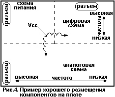
Example of good component placement
Figure 4 shows a possible layout of all components on the board, including the power supply. This uses three separate and isolated ground/power planes: one for the source, one for the digital circuit, and one for the analog circuit. The ground and power circuits of the analog and digital parts are combined only in the power supply. High-frequency noise is filtered out in the power circuits by chokes. In this example, the high frequency signals of the analog and digital parts are separated from each other. This design has a very high probability of a favorable outcome, since it is ensured good accommodation components and following the rules of circuit separation.
There is only one case where it is necessary to combine analog and digital signals over the analog ground polygon area. Analog-to-digital and digital-to-analog converters are housed in housings with analog and digital ground pins. Taking into account the previous discussion, it can be assumed that the digital ground pin and analog ground pin should be connected to the digital and analog ground buses, respectively. However, in this case this is not true.
The names of the pins (analog or digital) refer only to the internal structure of the converter, to its internal connections. In the circuit, these pins must be connected to the analog ground bus. The connection can also be made inside an integrated circuit, but achieving low resistance of such a connection is quite difficult due to topological restrictions. Therefore, when using converters it is assumed outer join analog and digital ground pins. If this is not done, then the parameters of the microcircuit will be significantly worse than those given in the specification.
It must be taken into account that the digital elements of the converter can degrade the quality characteristics of the circuit by introducing digital noise into the analog ground and analog power circuits. When designing converters, this negative impact is taken into account so that the digital part consumes as little power as possible. At the same time, interference from switching logic elements is reduced. If the digital pins of the converter are not heavily loaded, then internal switching usually does not cause any special problems. When designing a PCB containing an ADC or DAC, careful consideration must be given to decoupling the converter's digital power supply to analog ground.
FREQUENCY CHARACTERISTICS OF PASSIVE COMPONENTS
Correct selection of passive components is essential for proper operation of analog circuits. Start your design by carefully considering the high-frequency characteristics of passive components and preliminary placement and layout of them on the board sketch.
A large number of designers completely ignore the frequency limitations of passive components when used in analog circuitry. These components have limited frequency ranges and operating them outside the specified frequency range can lead to unpredictable results. Some may think that this discussion only concerns high-speed analog circuits. However, this is far from true - high-frequency signals have a strong impact on the passive components of low-frequency circuits through radiation or direct communication through conductors. For example, a simple low-pass filter on an op-amp can easily become a high-pass filter when exposed to high frequency at its input.
Resistors
The high-frequency characteristics of resistors can be represented by the equivalent circuit shown in Figure 5.

There are three types of resistors commonly used: 1) wirewound, 2) carbon composite, and 3) film. It doesn't take much imagination to understand how a wirewound resistor can be converted into an inductance, since it is a coil of wire made of high-resistance metal. Most developers electronic devices have no idea about the internal structure of film resistors, which are also a coil, albeit made of a metal film. Therefore, film resistors also have an inductance that is less than that of wirewound resistors. Film resistors with a resistance of no more than 2 kOhm can be freely used in high frequency circuits Oh. The resistor terminals are parallel to each other, so there is a noticeable capacitive coupling between them. For high resistance resistors, the terminal capacitance will reduce the total impedance by high frequencies.
Capacitors
The high-frequency characteristics of capacitors can be represented by the equivalent circuit shown in Figure 6.

Capacitors in analog circuits are used as decoupling and filtering components. For an ideal capacitor, the reactance is determined by the following formula:

Therefore, a 10 µF electrolytic capacitor will have a resistance of 1.6 ohms at 10 kHz and 160 µohms at 100 MHz. Is it so?
When using electrolytic capacitors, care must be taken correct connection. The positive terminal must be connected to a more positive constant potential. An incorrect connection causes DC current to flow through the electrolytic capacitor, which can damage not only the capacitor itself, but also part of the circuit.
In rare cases, the DC potential difference between two points in the circuit may change its sign. This requires the use of non-polar electrolytic capacitors, the internal structure of which is equivalent to two polar capacitors connected in series.
Inductance
The high-frequency characteristics of inductances can be represented by the equivalent circuit shown in Figure 7.
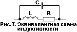
Inductance reactance is described by the following formula:
![]()
Therefore, a 10 mH inductance will have a reactance of 628 ohms at 10 kHz, and a reactance of 6.28 megohms at 100 MHz. Right?
Printed circuit board
The printed circuit board itself has the characteristics of the passive components discussed above, although not so obvious.
The pattern of conductors on a printed circuit board can be both a source and a receiver of interference. Good wiring reduces the sensitivity of the analog circuit to radiation sources.
The printed circuit board is susceptible to radiation because the conductors and leads of the components form a kind of antenna. Antenna theory is a rather complex subject to study and is not covered in this article. However, some basics are provided here.
A bit of antenna theory
On DC or low frequencies the active component predominates. As the frequency increases, the reactive component becomes more and more significant. In the range from 1 kHz to 10 kHz, the inductive component begins to take effect and the conductor is no longer a low-impedance connector, but rather acts as an inductor.
The formula for calculating the inductance of a PCB conductor is as follows:
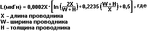
Typically, traces on a printed circuit board have values from 6 nH to 12 nH per centimeter of length. For example, a 10 cm conductor has a resistance of 57 mOhm and an inductance of 8 nH per cm. At a frequency of 100 kHz, the reactance becomes 50 mOhm, and at higher frequencies the conductor will be an inductance rather than a resistive one.
The rule for a whip antenna is that it begins to noticeably interact with the field at about 1/20 of the wavelength, and maximum interaction occurs at a rod length of 1/4 of the wavelength. Therefore, the 10 cm conductor from the example in the previous paragraph will start to become a pretty good antenna at frequencies above 150 MHz. It must be remembered that despite the fact that the clock generator of a digital circuit may not operate at frequencies above 150 MHz, higher harmonics are always present in its signal. If the printed circuit board contains components with pin pins of considerable length, then such pins can also serve as antennas.
The other main type of antenna is loop antenna. The inductance of a straight conductor increases greatly when it bends and becomes part of an arc. Increasing inductance lowers the frequency at which the antenna begins to interact with the field lines.
Experienced PCB designers with a reasonable understanding of loop antenna theory know not to design loops for critical signals. Some designers, however, do not think about this, and the return and signal current conductors in their circuits are loops. The creation of loop antennas is easy to demonstrate with an example (Fig. 8). In addition, the creation of a slot antenna is shown here.

Let's consider three cases:
Option A is an example of bad design. It does not use an analog ground polygon at all. The loop circuit is formed by the ground and signal conductors. When a current passes, an electric field and a magnetic field perpendicular to it arise. These fields form the basis loop antenna. The loop antenna rule states that for best efficiency, the length of each conductor should be equal to half the wavelength of the received radiation. However, it should be remembered that even at 1/20 of the wavelength, the loop antenna is still quite effective.
Option B better option A, but there is a gap in the polygon, probably to create a specific place for routing signal conductors. The signal and return current paths form a slot antenna. Other loops form in the cutouts around the chips.
Option B is an example of a better design. The signal and return current paths coincide, negating the effectiveness of the loop antenna. Note that this design also has cutouts around the chips, but they are separated from the return current path.
The theory of signal reflection and matching is close to the theory of antennas.
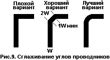
When the PCB conductor is rotated through an angle of 90°, signal reflection may occur. This is mainly due to changes in the width of the current path. At the apex of the corner, the trace width increases by 1.414 times, which leads to a mismatch in the characteristics of the transmission line, especially the distributed capacitance and the trace's own inductance. Quite often it is necessary to rotate a trace on a printed circuit board by 90°. Many modern CAD packages allow you to smooth the corners of drawn routes or draw routes in the form of an arc. Figure 9 shows two steps to improve the corner shape. Only the last example maintains a constant path width and minimizes reflections.
Tip for experienced PCB designers: leave the smoothing process for the last stage of work before creating teardrop-shaped pins and filling polygons. Otherwise, the CAD package will take longer to smooth due to more complex calculations.
Capacitive coupling occurs between PCB conductors on different layers when they intersect. Sometimes this can create a problem. Conductors placed one above the other on adjacent layers create a long film capacitor. The capacity of such a capacitor is calculated using the formula shown in Figure 10.

For example, a printed circuit board may have the following parameters:
- 4 layers; the signal and ground polygon layers are adjacent,
- interlayer spacing - 0.2 mm,
- conductor width - 0.75 mm,
- conductor length - 7.5 mm.
The typical ER dielectric constant for FR-4 is 4.5.
Substituting all the values into the formula, we get a capacitance value between these two buses equal to 1.1 pF. Even such a seemingly small capacity is unacceptable for some applications. Figure 11 illustrates the effect of a 1 pF capacitance when connected to the inverting input of a high-frequency op-amp.

It can be seen that the amplitude of the output signal doubles at frequencies close to the upper limit of the frequency range of the op-amp. This, in turn, can lead to oscillation, especially at antenna operating frequencies (above 180 MHz).
This effect gives rise to numerous problems, for which there are, however, many ways to solve them. The most obvious of them is reducing the length of the conductors. Another way is to reduce their width. There is no reason to use a conductor of this width to connect the signal to the inverting input, because Very little current flows through this conductor. Reducing the length of the trace to 2.5 mm and the width to 0.2 mm will lead to a decrease in capacitance to 0.1 pF, and such capacitance will no longer lead to such a significant increase in the frequency response. Another solution is to remove part of the polygon under the inverting input and the conductor that goes to it.
The width of the PCB conductors cannot be reduced indefinitely. The limit width is defined as technological process, and the thickness of the foil. If two conductors pass close to each other, then a capacitive and inductive coupling is formed between them (Fig. 12).

Signal conductors should not be routed parallel to each other, except in the case of differential or microstrip lines. The gap between conductors should be at least three times the width of the conductors.
Capacitance between traces in analog circuits can create problems with large resistor values (several megohms). The relatively large capacitive coupling between the inverting and non-inverting inputs of an op-amp can easily cause the circuit to oscillate.
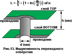
For example, with d=0.4 mm and h=1.5 mm (fairly common values), the inductance of the hole is 1.1 nH.
Remember that if there are large resistances in the circuit, then special attention should be paid to cleaning the board. During the final operations of manufacturing a printed circuit board, any remaining flux and contaminants must be removed. Recently, when installing printed circuit boards, water-soluble fluxes are often used. Being less harmful, they are easily removed with water. But at the same time, washing the board with insufficiently clean water can lead to additional contamination that worsens the dielectric characteristics. Therefore, it is very important to clean the high-impedance circuit board with fresh distilled water.
SIGNAL ISOLATION
As already noted, interference can penetrate into the analog part of the circuit through the power supply circuits. To reduce such interference, decoupling (blocking) capacitors are used to reduce the local impedance of the power buses.
If you need to lay out a printed circuit board that has both analog and digital parts, then you need to have at least a small understanding of the electrical characteristics of the logic elements.
A typical output stage of a logic element contains two transistors connected in series with each other, as well as between the power and ground circuits (Fig. 14).

These transistors ideally operate strictly in antiphase, i.e. when one of them is open, then at the same moment in time the second is closed, generating either a logical one or a logical zero signal at the output. In the steady state logic state, the power consumption of the logic element is small.
The situation changes dramatically when the output stage switches from one logic state to another. In this case, for a short period of time, both transistors can be open simultaneously, and the supply current of the output stage increases greatly, since the resistance of the current path from the power bus to the ground bus through two series-connected transistors decreases. The power consumption increases abruptly and then also decreases, which leads to a local change in the supply voltage and the occurrence of a sharp, short-term change in current. These changes in current result in the emission of radio frequency energy. Even on a relatively simple printed circuit board there may be tens or hundreds of considered output stages of logic elements, so the total effect of their simultaneous operation can be very large.
It is impossible to accurately predict the frequency range in which these current surges will occur, since the frequency of their occurrence depends on many factors, including the propagation delay of switching transistors of the logic element. The delay, in turn, also depends on many random reasons that arise during the production process. Switching noise has a broadband distribution of harmonic components over the entire range. To suppress digital noise There are several methods, the use of which depends on the spectral distribution of noise.
Table 2 shows the maximum operating frequencies for common capacitor types.
table 2
From the table it is obvious that tantalum electrolytic capacitors are used for frequencies below 1 MHz; at higher frequencies, ceramic capacitors should be used. It must be remembered that capacitors have their own resonance and their incorrect choice may not only not help, but also aggravate the problem. Figure 15 shows typical self-resonances of two common capacitors - 10 μF tantalum electrolytic and 0.01 μF ceramic.

Actual specifications may vary between different manufacturers and even from batch to batch within the same manufacturer. It is important to understand that for a capacitor to operate effectively, the frequencies it suppresses must be in a lower range than its own resonance frequency. Otherwise the character reactance will be inductive and the capacitor will no longer work effectively.
Do not be mistaken that one 0.1 µF capacitor will suppress all frequencies. Small capacitors (10 nF or less) can operate more efficiently at higher frequencies.
IC power decoupling
Decoupling the power supply of integrated circuits to suppress high-frequency noise consists of using one or more capacitors connected between the power and ground pins. It is important that the conductors connecting the leads to the capacitors are short. If this is not the case, then the self-inductance of the conductors will play a significant role and negate the benefits of using decoupling capacitors.
A decoupling capacitor must be connected to each chip package, regardless of whether there are 1, 2, or 4 op-amps inside the package. If the op amp is dual-supplied, then it goes without saying that decoupling capacitors should be located at each power pin. The capacitance value must be carefully selected depending on the type of noise and interference present in the circuit.
In particularly difficult cases, it may be necessary to add an inductance connected in series with the power output. The inductance should be located before, not after, the capacitors.
Another, cheaper way is to replace the inductance with a resistor with low resistance (10...100 Ohms). In this case, together with the decoupling capacitor, the resistor forms a low-pass filter. This method reduces the power supply range of the op-amp, which also becomes more dependent on power consumption.
Typically, to suppress low-frequency noise in power circuits, it is sufficient to use one or more aluminum or tantalum electrolytic capacitors at the power input connector. An additional ceramic capacitor will suppress high-frequency interference from other boards.
ISOLATION OF INPUT AND OUTPUT SIGNALS
Many noise problems result from directly connecting input and output pins. As a result of the high-frequency limitations of passive components, the response of a circuit when exposed to high-frequency noise can be quite unpredictable.
In a situation where the frequency range of the induced noise is significantly different from the frequency range of the circuit, the solution is simple and obvious - placing a passive RC filter to suppress high-frequency interference. However, when using a passive filter, you must be careful: its characteristics (due to the non-ideal frequency characteristics of passive components) lose their properties at frequencies 100...1000 times higher than the cutoff frequency (f 3db). When using series-connected filters tuned to different frequency ranges, the higher frequency filter should be closest to the source of interference. Ferrite ring inductors can also be used to suppress noise; they retain the inductive nature of the resistance up to a certain frequency, and above their resistance becomes active.
Tips on analog circuit can be so large that it is only possible to get rid of (or at least reduce) them through the use of screens. To operate effectively, they must be carefully designed so that the frequencies producing biggest problems, could not get into the scheme. This means that the screen should not have holes or cutouts larger than 1/20 of the wavelength of the radiation being screened. It is a good idea to allocate sufficient space for the proposed shield from the very beginning of the PCB design. When using a shield, you can optionally use ferrite rings (or beads) for all connections to the circuit.
OPERATIONAL AMPLIFIER CASES
One, two, or four operational amplifiers are usually placed in one package (Fig. 16).
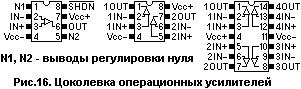
A single op amp often also has additional inputs, for example to adjust the offset voltage. Dual and quad op amps have only inverting and non-inverting inputs and output. Therefore, if it is necessary to have additional adjustments, it is necessary to use single operational amplifiers. When using additional outputs, you must remember that by their structure they are auxiliary inputs, so they must be controlled carefully and in accordance with the manufacturer's recommendations.
In a single op amp, the output is located on the opposite side of the inputs. This can make it difficult to operate the amplifier at high frequencies due to the long feedback lines. One way to overcome this is to place the amplifier and feedback components on different sides of the PCB. This, however, results in at least two additional holes and cuts in the ground polygon. Sometimes it is worth using a dual op amp to solve this problem, even if the second amplifier is not used (and its pins must be connected properly). Figure 17 illustrates the reduction in the length of the feedback circuit conductors for an inverting connection.

Dual op amps are especially common in stereo amplifiers, and quad op amps are used in multistage filter circuits. However, there is a rather significant disadvantage to this. Even though modern technology provides decent isolation between amplifier signals on the same silicon chip, there is still some crosstalk between them. If it is necessary to have a very small amount of such interference, then it is necessary to use single operational amplifiers. Crosstalk does not only occur when using dual or quad amplifiers. Their source can be the very close proximity of passive components of different channels.
Dual and quad op-amps, in addition to the above, allow for more dense installation. The individual amplifiers appear to be mirror-image relative to each other (Fig. 18).

Figures 17 and 18 do not show all connections required for normal operation, for example, a mid-level shaper with unipolar power supply. Figure 19 shows a diagram of such a shaper when using a quad amplifier.

The diagram shows all necessary connections to implement three independent inverting stages. It is necessary to pay attention to the fact that the conductors of the half-supply voltage driver are located directly under the integrated circuit housing, which makes it possible to reduce their length. This example illustrates not what should be, but what should be done. The average level voltage, for example, could be the same for all four amplifiers. Passive components can be sized accordingly. For example, frame size 0402 planar components match the pin spacing of a standard SO package. This allows conductor lengths to be kept very short for high frequency applications.
3D AND SURFACE MOUNTING
When placing op amps in DIP packages and passive components with lead wires, vias must be provided on the printed circuit board to mount them. Such components are currently used when there are no special requirements for the dimensions of the printed circuit board; They are usually cheaper, but the cost of the printed circuit board increases during the manufacturing process due to drilling additional holes for component leads.
In addition, when using external components, the dimensions of the board and the length of the conductors increase, which does not allow the circuit to operate at high frequencies. Vias have their own inductance, which also limits the dynamic characteristics of the circuit. Therefore, overhead components are not recommended for implementing high-frequency circuits or for analog circuits located close to high-speed logic circuits.
Some designers, trying to reduce the length of the conductors, place resistors vertically. At first glance it may seem that this shortens the length of the route. However, this increases the path of current through the resistor, and the resistor itself represents a loop (turn of inductance). The emitting and receiving ability increases many times over.
Surface mounting does not require a hole for each component lead. However, problems arise when testing the circuit, and you have to use vias as control points, especially when using small-sized components.
UNUSED OP-AMP SECTIONS
When using dual and quad op-amps in a circuit, some sections may remain unused and must be connected correctly in this case. Incorrect connections can lead to increased power consumption, more heat, and more noise from the op amps used in the same package. The pins of unused operational amplifiers can be connected as shown in Fig. 20a. Connecting pins with additional components(Fig. 20b) will make it easy to use this op-amp during setup.

CONCLUSION
Remember the following basic points and keep them in mind at all times when designing and wiring analog circuits.
Are common:
- think of the PCB as a component electrical diagram;
- have an awareness and understanding of sources of noise and interference;
- model and layout circuits.
Printed circuit board:
- use printed circuit boards only from quality material(eg FR-4);
- circuits made on multilayer printed circuit boards are 20 dB less susceptible to external interference than circuits made on double-layer boards;
- use separated, non-overlapping polygons for different lands and feeds;
- Place the ground and power polygons on the inner layers of the PCB.
Components:
- Be aware of the frequency limitations introduced by passive components and board traces;
- try to avoid vertical placement of passive components in high-speed circuits;
- For high-frequency circuits, use components designed for surface mounting;
- conductors should be shorter, the better;
- if a larger conductor length is required, then reduce its width;
- Unused pins of active components must be connected correctly.
Wiring:
- place the analog circuit near the power connector;
- never route conductors transmitting logic signals through the analog area of the board, and vice versa;
- make the conductors suitable for the inverting input of the op-amp short;
- make sure that the conductors of the inverting and non-inverting inputs of the op-amp are not located parallel to each other over a long distance;
- try to avoid using extra vias, because... their own inductance can lead to additional problems;
- do not route the conductors at right angles and smooth the tops of the corners if possible.
Interchange:
- use the correct types of capacitors to suppress noise in power supply circuits;
- to suppress low-frequency interference and noise, use tantalum capacitors at the power input connector;
- To suppress high-frequency interference and noise, use ceramic capacitors at the power input connector;
- use ceramic capacitors at each power pin of the microcircuit; if necessary, use several capacitors for different frequency ranges;
- if excitation occurs in the circuit, then it is necessary to use capacitors with a lower capacitance value, and not a larger one;
- in difficult cases, use series-connected resistors of low resistance or inductance in power circuits;
- Analog power decoupling capacitors should only be connected to the analog ground, not the digital ground.
- Minimize RF bus lengths
- Separate the power and ground buses between the analog and digital parts of the circuit
- Do not break earth polygons with high-frequency conductors
Definitions:
Electromagnetic compatibility (EMC): the ability, during operation, not to make an excessive contribution to the environment through electromagnetic radiation. When this condition is met, all electronic components work together correctly.
Electromagnetic interference (EMI): electromagnetic energy, emitted by one device, which can lead to a violation of the quality characteristics of another device.
Electromagnetic immunity, EMPU (Electromagnetic immunity, or susceptibility, EMS): tolerance (resistance) to the effects of electromagnetic energy.
Designing for EMC: 4 Key Rules
The problem with rules: the more rules you have, the harder it is to follow them all. The prioritization of their implementation is different.
Suppose, when creating a multilayer printed circuit board, you need to route a high-frequency signal from an analog component to a digital one. Naturally, you want to minimize the likelihood of an electromagnetic compatibility (EMC) problem. After searching the Internet, you find three recommendations that seem to be relevant to your situation:
Your vision of three possible wiring options is shown in Fig. 1.
In the first case, the routes are routed directly between the two components, and the ground polygon remains continuous. In the second case, a gap is formed in the polygon, and the tracks pass across this gap. In the third case, the routes are laid along the gap in the polygon.
In each of these three cases, one of the above rules is violated. Are these alternative cases equally good because they satisfy two of the three rules? Are they all bad because they each break at least one rule?
These are the questions PCB designers face every day. The right or wrong choice of routing strategy can lead to results in which the board either meets all EMC requirements or has problems with susceptibility to external signals. In this case the choice should be clear, but we will come back to this later
The problems are reduced after the recommendations are prioritized. Design guidelines are only useful if they are well understood and if they form part of a complete strategy. Once designers learn to prioritize guidelines and understand how those guidelines should be used, they can skillfully design good PCBs.
The following are the four main EMC rules based on general features electronics products. In many cases, PCB designers deliberately break one of these rules in an attempt to fulfill more important ones.
Rule 1: Minimize Signal Current Path
This simple rule appears in almost every list of EMC recommendations, but often it is either ignored or downplayed in favor of other recommendations.
Often the PCB designer doesn't even think about where the signal currents flow and prefers to think about signals in terms of voltage, but should be thinking in terms of current.
There are two axioms that every PCB designer should know:
- signal currents always return to their source, i.e. the current path is a loop
- signal currents always use the path with minimal impedance
At frequencies of several megahertz and above, the signal current path is relatively easy to determine because the path with minimum impedance is, in general, the path with minimum inductance. In Fig. Figure 2 shows two components on a printed circuit board. A 50 MHz signal travels along a conductor over the test site from component A to component B.

We know that the same magnitude of signal must propagate back from component B to component A. Let's assume that this current (let's call it return) flows from the terminal of component B, designated GND, to the terminal of component A, also designated GND.
Since the integrity of the polygon is ensured, and the terminals, designated as GND, of both components are located close to each other, this leads to the conclusion that the current will take the shortest path between them (path 1). However, this is not correct. High frequency currents choose the path of least inductance (or the path with the minimum loop area, the path of smallest turn). Most of the signal return current flows through the polygon in a narrow path just below the signal trace (path 2).
If the polygon was made for some reason with a cutout as shown in Figure 3, then cutout 1 would have little effect on signal integrity and emission. Another cutout 2 may lead to significant problems; it conflicts with recommendation 2. The loop area increases significantly; the reverse currents are so intense that they flow along the discontinuity boundary.

At low frequencies (generally kHz and below), the path of lowest impedance tends to be the path with the lowest signal frequency.

For a PCB with solid return current polygons, the polygon resistance tends to dissipate the current so that current flowing between two distant points can be distributed over a larger area of the board, as shown in Figure 4.

On a mixed-signal board with low-frequency analog and digital components, this can be a problem. Figure 5 illustrates how a well-placed rupture in an earthen landfill can correct the situation by capturing low frequency return currents flowing through the landfill in a designated area.
Rule 2. Do not subdivide the return signal polygon
One view is that the analog return signal current should always be isolated from the digital return signal current.
This idea originated when analog and digital circuits operated at kilohertz frequencies. For example, boards that were used for digital audio often experienced noise problems due to the influence of low-frequency digital signal currents traveling under the area of the board where sensitive analog amplifiers were located. Some time ago, audio designers tried to avoid this problem by separating return current polygons to control return paths and removing analog current circuits from digital ones.
Our students are asked to solve a design problem that requires protecting sensitive analog components (usually audio amplifiers or phase-locked oscillators) from the digital portion of the circuit by separating the return signal current polygon in such a way that the LF currents are isolated and the HF currents are not generated. interference It is usually not obvious how this can be accomplished, and quite often breaks in polygons create more problems than they solve.
A similar situation arises when wiring tires of automobile or aviation electronic equipment. In such equipment, the digital circuit return currents are often isolated from the general enclosure in order to protect the digital circuits from damage by large LF currents that may flow through the metal structure of the vehicle.
Undoubtedly, there are situations where a well-placed break in the return current polygon is required. However, the most reliable method is one continuous polygon for all return signal currents. In cases where a single low-frequency signal is susceptible to interference (capable of mixing with other signals on the board), routing is used on a separate layer to return this current to the source. In general, never use splitting or cutting in the return signal current polygon. If you are still convinced that a cutout in the polygon is necessary to solve the problem of low-frequency isolation, consult an expert. Do not rely on design recommendations or applications, or try to implement a design that has worked for someone else in a similar design.
Now that we are familiar with the two main rules of EMC, we are ready to revisit the problem in Fig. 1. Which of the alternatives is the best? The first one is the only one that does not contradict the rules.
If for some reason (beyond the design desires) a gap in the earthen area was required, then the third wiring option is more acceptable. Tracing along the discontinuity minimizes the signal current loop area.
Rule 3: Do not place high-speed circuits between connectors
This is one of the most common problems among the board designs we have reviewed and evaluated in our lab. In simple boards that should not have any failures under all EMC requirements without any additional cost or effort, good shielding and filtering were negated because this simple rule was broken.
Why is connector placement so important? At frequencies below several hundred megahertz, the wavelength is on the order of a meter or more. The conductors on the board - possible antennas - have a relatively short electrical length and therefore work inefficiently. However, cables or other devices connected to the board can be quite effective antennas.
However, high-speed circuit elements placed between connectors can easily create potential differences between the connectors of several millivolts or more. These voltages can induce excitation currents into connected cables, increasing their emissions.
A board that meets all the specifications when the connectors are located on one edge can become an EMC engineer's nightmare if even one connector with a cable attached is located on the opposite side of the board. Products that exhibit this type of problem (cables carrying voltages induced through an entire polygon) are particularly difficult to restore to normal. Often this requires fairly good shielding. In many cases, this shielding would be completely unnecessary if the connectors were located on one side or in a corner of the board.
Rule 4. Transition time of the control signal
Board running on clock frequency 100 MHz should never meet the requirements when operating at 2 GHz. A well-formed digital signal will have more power on the lower harmonics and not much power on the higher ones. By controlling the signal transition time, it is possible to control the signal power at higher harmonics, which is preferable for EMC. Excessively long transient times can lead to signal integrity problems and thermal problems. During the development and design process, a compromise must be made between these competing necessary conditions. Transition time equal to approximately 20% of signal period
, results in an acceptable waveform, reducing problems arising from crosstalk and radiation. Depending on the application, the transition time may be more or less than 20% of the signal period; however, this time should not be uncontrollable.
There are three main ways to change the edges of digital signals: - use of digital series chips
, the speed of which coincides with the required speed,
- placing a resistor or inductor on the ferrite in series with the output signal, and
The first method is often the simplest and most effective.
Using a resistor or ferrite gives the designer greater transient control and less impact on changes that occur in logic families over time. The advantage of using a control capacitor is that it can be easily removed when not needed. However, it must be remembered that capacitors increase the current of the RF signal source.
Note that trying to filter a single-wire signal in the return current path is always a bad idea. For example, never route a low-frequency trace across a gap in the return polygon in an attempt to filter out high-frequency noise. After looking at the first two rules, this should be obvious. However, boards using this incorrect strategy are sometimes identified in our laboratory.
Generally speaking, during the board design and layout process, priorities need to be set to comply with EMC regulations. These rules should not be compromised in attempts to follow other EMC recommendations. However, there are several additional recommendations that are worth considering. For example, it is important to provide adequate power bus separation, keep I/O traces short, and provide filtering for output signals. It's also a good idea to choose your active devices carefully. Not all pin-compatible semiconductor components are equivalent in terms of noise. Two devices with the same technical parameters, but made by different manufacturers, can differ significantly in the noise they create at the input and output pins, as well as at the power pins. This is especially true for highly integrated chips such as microprocessors and large application-specific applications.
integrated circuits
Whose advice can you trust? Trust anyone whose recommendations clearly help you fulfill the four main rules. A little extra care during design can save a lot of time, money and effort that would be wasted trying to get an otherwise intractable product to work correctly.
Translation of the article:
Dr. Todd Hubing, Dr. Tom Van Doren
Designing for EMC: The TOP 4 GUIDELINES
Printed Circuit Design & Manufacture, June 2003
Dr. Todd Hubing, Distinguished Professor of Electrical and Computer Engineering, twice awarded the “Best Symposium Publications” prize from the International Symposium of the Institute of Electrical and Electronics Engineers.
Dr. Tom Van Doren, professor of electrical and computer engineering at the Electromagnetic Compatibility Laboratory at the University of Missouri-Rolla.
1. General Provisions
To prevent problems with electrostatics and noise, certain rules must be followed when laying out the printed circuit board. The most critical point is pin C, because it is connected to the built-in 3.3-volt power supply of the MK core. Therefore, the filter capacitor should be located as close to the terminal as possible.
You should also pay close attention to the wiring of the power and ground circuits. The food is supplied by a “star”. We recommend placing a layer of earth on the installation side directly under the MK body. The Vcc and Vss lines should have only one connection point with the rest of the circuit to avoid interference on the MK and from the MK. Filter capacitors (DeCaps) should be located as close as possible to the corresponding terminals. If they are removed too far, they cease to perform their function.
When using quartz resonators, they should be located at a minimum distance from the Xn(A) terminals.
If possible, it is advisable to place filter capacitors on the MK mounting side.
2 Power supply wiring
The Vcc and Vss buses need to be routed not in a series chain, but in a “star”. For Vss, an earthen polygon under the MK body is recommended, connected at one point to the rest of the circuit.
Below are two examples of bad and good power supply wiring.
3 Filtering output C


4 Filtering power circuits
Filter capacitors (DeCaps) for power circuits must be located in the path of power currents, otherwise their use does not make sense. The following figure explains this statement:


5 Location of the quartz resonator and wiring of signal circuits
Quartz should be located as close to the MK as possible. Thus, the generator capacitors will be located “behind” the quartz.


6 Additional documentation
For more detailed information, see the Application Note 16bit-EMC-Guideline.
7 List of MK conclusions
The table shows the MK conclusions that are critical to electromagnetic interactions and brief information about their connection.
| Output name | Function performed |
| Vcc | |
| Vss | Main power supply for the I/O ports of the MK core, next to the 3.3V internal regulator input, next to the crystal oscillator |
| WITH | External smoothing capacitor for the built-in 3.3V regulator used to power the MK core. Please note that this pin is the main source of noise. |
| AVcc* | ADC power supply |
| AVss* | ADC power supply |
| AVRL* | |
| AVRH* | ADC reference input |
| DVcc*, HVcc* | Power supply for high current PWM outputs, not connected to Vcc, must be connected to additional source nutrition. |
| DVss*, HVss* | Power supply for high current PWM outputs, with Vss not connected, must be connected to an additional power source. |
| X0, X0A* | Generator input. If not used, connect through a resistor to the “+” power supply or ground (see DS). |
| X1, X1A* | Generator output. Quartz resonator and the capacitor should be connected along the shortest path to pin X1. If not used, leave unconnected. |
* - may not be present in a specific MK
A little about the "rake" when designing boards.
The most typical error in wiring power circuits in many designs: the blocking capacitances along the “+” and “-” supply lines of the op-amp are thrown onto the ground layer far from each other, that is, the loop current consumption of the op-amp flows through the ground layer. These containers must be positioned so that the distance between the points of their connection to the earthen layer is minimal. High-frequency blocking - easily fits under DIP-8 housing SMD capacitors standard size 1206, and with some skill - 1210. Naturally, the area of the resulting current flow circuit should also be minimal, this goes without saying.
Resistors in the power circuits of each IC greatly simplify the wiring, because serve as jumpers and allow the “+” and “-” power supplies to be placed close to each other, which is highly desirable to reduce the emissions of signal/output currents from the power circuits.
There is also an elegant (but very labor-intensive) method for suppressing ground noise without explicitly separating the grounds, especially useful when using double-sided boards - maintaining as much as possible a solid layer of ground on one side (i.e., essentially single-layer circuit routing on the other side , with a minimum of “jumpers”), a thorough analysis of the contours of the flow of power currents along this ground plane and finding equipotential points, i.e. points, the potential difference between which, when currents flow through the ground in the power/load circuits, remains close to zero. These points are used as the “signal” ground pins. The type of current flow contours can be changed, if necessary, by introducing additional cuts or vice versa, by making jumpers in the sections of the earthen layer that arise according to the wiring conditions.
The most detailed study of issues of topology/current flow, etc. was carried out to create methods for designing devices that are resistant to EMP pulses that occur during the explosion of nuclear weapons or pulsed EMP generators. Unfortunately, publications on this topic are scattered, and moreover, they are often still “under the table.” I scanned one of the illustrative articles, but I can’t attach it here - the limit on the number of attachments has been selected.
About the design of PP.
It should be immediately noted that the sometimes straightforward approach - “the more layers the better” - does not work for purely analog (and partly digital) circuits. There are too many factors involved.
Single/double-layer PP on getinax/fiberglass without metallization of holes - currently only adequate for very simple devices in a large (>>10000) series. The main disadvantages are low reliability under harsh operating conditions (due to detachment of contact pads/conductors during mechanical vibrations and thermal cycles, accumulation of moisture/fluxes through the walls of holes), as well as complexity (and high cost) quality wiring of any complex circuits. The installation density is low (usually no more than 3...4 pins per square centimeter of the total board area). The advantage is extreme simplicity and low cost in production (with large volumes and design standards of the order of 0.38 mm - less than $0.3/sq. dm) due to the lack of metallization and the possibility of replacing drilling holes with punching them.
Requirements for increasing packing density while maintaining reliability in the production of BGA packages and portable equipment led to the development of microvia technology, when in addition to the usual (through) via holes on the board on one or both sides, blind via holes are formed (usually with a laser) to the underlying layer, metallized in one cycle with the metallization of through holes. The size of the contact pad for such a transition (0.2...0.3 mm) is much smaller than for a through hole, and the routing in the remaining layers is not disrupted. In addition, in some cases microvia can be placed on the contact pad of an SMD element without the risk of a noticeable part of the solder leaving the hole due to its small size and depth (no more than 0.1...0.15 mm). This greatly increases the wiring density, because conventional vias on pads SMD elements As a rule, it cannot be posted. Microvia can also be formed into the inner layers, but this is significantly more difficult and expensive to produce.
A few words about the thickness of copper and the coating of the boards. The main part of the boards is made on materials with foil thicknesses of 35, 18 and 9 microns, while during metallization of the holes on the outer layers, another 15-25 microns of copper are added (there should be ~ 20 microns in the holes). Boards with design standards of 0.127 or less, as a rule, are made on a material with a foil thickness of ~9 microns (the thinner the foil, the less distortion of the shape of the pattern due to lateral undercut of the conductors). There is no need to worry about the “small cross-section of copper”, because Printed conductors, due to good cooling, allow much higher current densities (~ 100 A/sq. mm) than the mounting wire (3...10 A/sq. mm). The final thickness in the outer layers, due to the deposition of copper during metallization of the holes, naturally turns out to be greater than that of the original foil. The resistance of flat conductors depends on their plan geometry according to a simple law: resistance of a square x number of squares. The resistance of a square does not depend on its absolute size, but only on the thickness and conductivity of the material. That is, the resistance of a conductor with a width of 0.25 mm and a length of 10 mm (i.e. 40 squares) is the same as with a width of 2.5 and a length of 100. For 35 micron copper foil this is about 0.0005 Ohm/square. On industrial boards, when metalizing holes on foil, an additional layer of copper is built up, so that the resistance of the square drops by another 20 percent compared to the above. Maintenance, even “fat”, has little effect on the resistance; its purpose is to increase the heat capacity of the conductors so that they do not burn out from short-term shock current. By using photomask correction (i.e., introducing corrections for undercuts) and anisotropic etching, manufacturers are able to produce boards with a thickness of the original foil up to 30-40% of the design standards, i.e. when using the thickest foil 105 microns (and taking into account copper deposition - somewhere around 125-130 microns), design standards can be from 0.3...0.35 mm.
A more significant limitation for power circuits is that the permissible current passed through the via hole depends mainly on its diameter, since the thickness of the metallization in it is small (15...25 μm) and, as a rule, does not depend on the thickness of the foil . For a hole with a diameter of 0.5 mm with a board thickness of 1.5 mm, the permissible current is about 0.4 A, for 1 mm - approximately 0.75 A. If it is necessary to pass more current through via holes, a rational solution would be to use not one large, but a set of small via holes, especially if they are dense placement in a “checkerboard” or “honeycomb” pattern - at the vertices of a grid of hexagons. Duplicating vias also provides a benefit in reliability, so it is often used in critical circuits (including signal circuits) when developing equipment for particularly critical applications (for example, life support systems).
Coatings of board conductors can be insulating and/or protective. A “solder mask” is a protective insulating coating in which windows are formed at the contact pads. The conductors can be left copper, or covered with a layer of metal that protects them from corrosion (tin/solder, nickel, gold, etc.). Each type of coating has advantages and disadvantages. Coatings can be thin-layer, a fraction of a micron thick (usually chemical), and thick-layer (galvanic, hot tinning). It is best to apply a solder mask to bare copper or a thin-layer coating; when applied to tinned traces, it holds worse and during soldering a capillary effect appears - solder wicking/mask separation. Gold plating comes in both types, chemical (thin) and galvanic (requiring electrical connection conductors, for example, on a connector). IN large-scale production Also popular is the option of coating pure copper (untinned) contact pads of boards with a flux-like varnish (organic coating). The choice of coating type depends on the installation technology and type of parts. For manual installation (and automatic for parts of standard size 0805 and larger), in the vast majority of cases, the best option is hot tinning of pads (HASL) with a copper mask. For smaller parts and automatic installation, if there are no requirements for particularly small leaks on the board, one of the best options is chemical (immersion) gold (Flash Gold) or immersion tin. Chemical gold is very cheap in the normal world, the same as hot tinning, and at the same time provides perfectly even seats for elements, without solder tubercles. However, when manufacturing circuit boards in the Russian Federation, it is often better to order coating not with immersion gold, but with tin - its solutions do not save as much. When soldering boards with thin coatings, including Flash Gold, they must be soldered quickly and/or filled with neutral flux to avoid oxidation of copper through the pores of the coating, and when automatically soldering, it is also advisable to use a neutral gas environment (nitrogen, freon).
Below is the most intelligible (in my opinion) literature on this issue, as well as an example of a two-layer computer board for a microprofile meter (profilometer) that I developed about 10 years ago, in which measures to ensure the quality of the topology were applied without fanaticism, only partially. However, this turned out to be enough that, without any shielding, in a working PC with its interference (and its own power part - control commutator motor) provide a resolution of several atoms, many times exceeding the requirements of the technical specifications (the op amps used are only TL084/LM324). The device was produced until very recently and was the only profilometer of class 1 accuracy in the Russian Federation.
Forum user: sia_2


