Discussions about television cameras. What is a CCD matrix
General information about CCD matrices.Currently, most image capture systems use CCD (charge-coupled device) matrices as the photosensitive device.
The operating principle of a CCD matrix is as follows: a matrix of photosensitive elements (accumulation section) is created on the basis of silicon. Each photosensitive element has the property of accumulating charges proportional to the number of photons hitting it. Thus, over some time (exposure time) the accumulation section produces a two-dimensional matrix of charges proportional to the brightness of the original image. The accumulated charges are initially transferred to the storage section, and then line by line and pixel by pixel to the output of the matrix.
The size of the storage section in relation to the accumulation section varies:
- per frame (matrices with frame transfer for progressive scan);
- per half-frame (matrices with frame transfer for interlaced scanning);
There are also matrices in which there is no storage section, and then the row transfer is carried out directly through the accumulation section. Obviously, for such matrices to work, an optical shutter is required.
The quality of modern CCD matrices is such that the charge remains virtually unchanged during the transfer process.
Despite the apparent variety of television cameras, the CCD matrices used in them are practically the same, since mass and large-scale production of CCD matrices is carried out by only a few companies. These are SONY, Panasonic, Samsung, Philips, Hitachi Kodak.
The main parameters of CCD matrices are:
- dimension in pixels;
- physical size in inches (2/3, 1/2, 1/3, etc.). Moreover, the numbers themselves do not determine the exact size of the sensitive area, but rather determine the class of the device;
- sensitivity.
Resolution of CCD cameras.
The resolution of CCD cameras is mainly determined by the size of the CCD matrix in pixels and the quality of the lens. To some extent, this can be influenced by the camera’s electronics (if it’s poorly made, it can worsen the resolution, but they rarely do anything frankly bad these days).
It is important to make one note here. In some cases, high-frequency spatial filters are installed in cameras to improve apparent resolution. In this case, an image of an object obtained from a smaller camera may appear even sharper than an image of the same object obtained objectively from a better camera. Of course, this is acceptable when the camera is used in visual surveillance systems, but it is completely unsuitable for constructing measurement systems.
Resolution and format of CCD matrices.
Currently, various companies produce CCD matrices covering a wide range of dimensions from several hundred to several thousand. This is how a matrix with a dimension of 10000x10000 was reported, and this message noted not so much the problem of the cost of this matrix as the problem of storing, processing and transmitting the resulting images. As we know, matrices with dimensions up to 2000x2000 are now more or less widely used.
The most widely, or more precisely, mass-used CCD matrices certainly include matrices with a resolution oriented to the television standard. These are matrices mainly of two formats:
- 512*576;
- 768*576.
Matrices 768*576 (sometimes a little more, sometimes a little less) allow you to get the maximum resolution for a standard television signal. At the same time, unlike matrices of the 512*576 format, they have a grid arrangement of photosensitive elements close to a square, and, therefore, equal horizontal and vertical resolution.
Often, camera manufacturers indicate resolution in television lines. This means that the camera allows you to see N/2 dark vertical strokes on a light background, arranged in a square inscribed in the image field, where N is the declared number of television lines. In relation to a standard television table, this assumes the following: by selecting the distance and focusing the table image, it is necessary to ensure that the upper and lower edges of the table image on the monitor coincide with the outer contour of the table, marked by the vertices of black and white prisms; then, after final subfocusing, the number is read in the place of the vertical wedge where the vertical strokes for the first time cease to be resolved. The last remark is very important because... and in the image of test fields of a table with 600 or more lines, alternating stripes are often visible, which, in fact, are moiré formed by the beating of the spatial frequencies of the lines of the table and the grid of sensitive elements of the CCD matrix. This effect is especially pronounced in cameras with high-frequency spatial filters (see above)!
I would like to note that, all other things being equal (this can mainly be influenced by the lens), the resolution of black-and-white cameras is uniquely determined by the size of the CCD matrix. So a 768*576 format camera will have a resolution of 576 television lines, although in some prospectuses you can find a value of 550, and in others 600.
Lens.
The physical size of the CCD cells is the main parameter that determines the requirement for the resolution of the lens. Another such parameter may be the requirement to ensure the operation of the matrix under light overload conditions, which will be discussed below.
For a 1/2 inch SONY ICX039 matrix, the pixel size is 8.6µm*8.3µm. Therefore, the lens must have a resolution better than:
1/8.3*10e-3= 120 lines (60 pairs of lines per millimeter).
For lenses made for 1/3-inch matrices, this value should be even higher, although this, oddly enough, does not affect the cost and such a parameter as aperture, since these lenses are made taking into account the need to form an image on a smaller light-sensitive field of the matrix. It also follows that lenses for smaller matrices are not suitable for large matrices due to significantly deteriorating characteristics at the edges of large matrices. At the same time, lenses for large sensors can limit the resolution of images obtained from smaller sensors.
Unfortunately, with all the modern abundance of lenses for television cameras, it is very difficult to obtain information on their resolution.
In general, we do not often select lenses, since almost all of our Customers install video systems on existing optics: microscopes, telescopes, etc., so our information about the lens market is in the nature of notes. We can only say that the resolution of simple and cheap lenses is in the range of 50-60 pairs of lines per mm, which is generally not enough.
On the other hand, we have information that special lenses produced by Zeiss with a resolution of 100-120 line pairs per mm cost more than $1000.
So, when purchasing a lens, it is necessary to conduct preliminary testing. I must say that most Moscow sellers provide lenses for testing. Here it is once again appropriate to recall the moire effect, the presence of which, as noted above, can mislead regarding the resolution of the matrix. So, the presence of moire in the image of sections of the table with strokes above 600 television lines in relation to the lens indicates a certain reserve of the latter’s resolution, which, of course, does not hurt.
One more, perhaps important note for those who are interested in geometric measurements. All lenses have distortion to one degree or another (pincushion-shaped distortion of the image geometry), and the shorter the lens, the greater these distortions, as a rule, are. In our opinion, lenses with focal lengths greater than 8-12 mm have acceptable distortion for 1/3" and 1/2" cameras. Although the level of “acceptability”, of course, depends on the tasks that the television camera must solve.
Resolution of image input controllers
The resolution of image input controllers should be understood as the conversion frequency of the analog-to-digital converter (ADC) of the controller, the data of which is then recorded in the controller’s memory. Obviously, there is a reasonable limit to increasing the digitization frequency. For devices that have a continuous structure of the photosensitive layer, for example, vidicons, the optimal digitization frequency is equal to twice the upper frequency of the useful signal of the vidicon.
Unlike such light detectors, CCD matrices have a discrete topology, so the optimal digitization frequency for them is determined as the shift frequency of the output register of the matrix. In this case, it is important that the controller’s ADC operates synchronously with the output register of the CCD matrix. Only in this case can the best conversion quality be achieved both from the point of view of ensuring a “rigid” geometry of the resulting images and from the point of view of minimizing noise from clock pulses and transient processes.
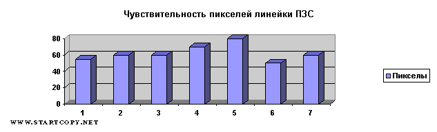
Sensitivity of CCD cameras
Since 1994, we have been using SONY card cameras in our devices based on the ICX039 CCD matrix. The SONY description for this device indicates a sensitivity of 0.25 lux on an object with a lens aperture of 1.4. Several times already, we have come across cameras with similar parameters (size 1/2 inch, resolution 752*576) and with a declared sensitivity of 10 or even 100 times greater than that of “our” SONY.
We checked these numbers several times. In most cases, in cameras from different companies, we found the same ICX039 CCD matrix. Moreover, all the “piping” microcircuits were also SONY-made. And comparative testing showed almost complete identity of all these cameras. So what's the question?
And the whole question is at what signal-to-noise ratio (s/n) the sensitivity is determined. In our case, the SONY company conscientiously showed sensitivity at s/n = 46 dB, while other companies either did not indicate this or indicated it in such a way that it is unclear under what conditions these measurements were made.
This is, in general, a common scourge of most camera manufacturers - not specifying the conditions for measuring camera parameters.
The fact is that as the requirement for the S/N ratio decreases, the sensitivity of the camera increases in inverse proportion to the square of the required S/N ratio:
Where:
I - sensitivity;
K - conversion factor;
s/n - s/n ratio in linear units,
Therefore, many companies are tempted to indicate camera sensitivity at a low S/N ratio.
We can say that the ability of matrices to “see” better or worse is determined by the number of charges converted from photons incident on its surface and the quality of delivery of these charges to the output. The amount of accumulated charges depends on the area of the photosensitive element and the quantum efficiency of the CCD matrix, and the quality of transportation is determined by many factors, which often come down to one thing - readout noise. The readout noise for modern matrices is on the order of 10-30 electrons or even less!
The areas of the elements of CCD matrices are different, but the typical value for 1/2 inch matrices for television cameras is 8.5 µm * 8.5 µm. An increase in the size of the elements leads to an increase in the size of the matrices themselves, which increases their cost not so much due to the actual increase in the production price, but due to the fact that the serial production of such devices is several orders of magnitude smaller. In addition, the area of the photosensitive zone is affected by the topology of the matrix to the extent that the percentage of the total surface of the crystal is occupied by the sensitive area (fill factor). In some special matrices, the fill factor is stated to be 100%.
Quantum efficiency (how much on average the charge of a sensitive cell in electrons changes when one photon falls on its surface) for modern matrices is 0.4-0.6 (for some matrices without anti-blooming it reaches 0.85).
Thus, it can be seen that the sensitivity of CCD cameras, related to a certain S/N value, has come close to the physical limit. According to our conclusion, typical sensitivity values of cameras for general use at s/w = 46 lie in the range of 0.15-0.25 lux of illumination on the object with a lens aperture of 1.4.
In this regard, we do not recommend blindly trusting the sensitivity figures indicated in the descriptions of television cameras, especially when the conditions for determining this parameter are not given and, if you see in the passport of a camera costing up to $500 a sensitivity of 0.01-0.001 lux in television mode, then before you are an example of, to put it mildly, incorrect information.
About ways to increase the sensitivity of CCD cameras
What do you do if you need to image a very faint object, such as a distant galaxy?One way to solve this is to accumulate images over time. The implementation of this method can significantly increase the sensitivity of the CCD. Of course, this method can be applied to stationary objects of observation or in cases where movement can be compensated, as is done in astronomy.
Fig1 Planetary nebula M57.
Telescope: 60 cm, exposure - 20 sec., temperature during exposure - 20 C.
At the center of the nebula there is a stellar object of magnitude 15.
The image was obtained by V. Amirkhanyan at the Special Astrophysical Observatory of the Russian Academy of Sciences.
It can be stated with reasonable accuracy that the sensitivity of CCD cameras is directly proportional to the exposure time.
For example, sensitivity at a shutter speed of 1 second relative to the original 1/50s will increase 50 times, i.e. it will be better - 0.005 lux.
Of course, there are problems along this path, and this is, first of all, the dark current of the matrices, which brings charges that accumulate simultaneously with the useful signal. The dark current is determined, firstly, by the manufacturing technology of the crystal, secondly, by the level of technology and, of course, to a very large extent by the operating temperature of the matrix itself.
Usually, to achieve long accumulation times, on the order of minutes or tens of minutes, the matrices are cooled to minus 20-40 degrees. C. The problem of cooling the matrices to such temperatures has been solved, but it is simply impossible to say that this cannot be done, since there are always design and operational problems associated with fogging of protective glasses and heat release from the hot junction of a thermoelectric refrigerator.
At the same time, technological progress in the production of CCD matrices has also affected such a parameter as dark current. Here the achievements are very significant and the dark current of some good modern matrices is very small. In our experience, cameras without cooling allow making exposures at room temperature within tens of seconds, and with dark background compensation up to several minutes. As an example, here is a photograph of the planetary nebula M57, obtained with the VS-a-tandem-56/2 video system without cooling with an exposure of 20 s.
The second way to increase sensitivity is the use of electron-optical converters (EOC). Image intensifiers are devices that enhance the luminous flux. Modern image intensifier tubes can have very large gain values, however, without going into details, we can say that the use of image intensifier tubes can only improve the threshold sensitivity of the camera, and therefore its gain should not be made too large.
Spectral sensitivity of CCD cameras

Fig.2 Spectral characteristics of various matrices
For some applications, the spectral sensitivity of the CCD is an important factor. Since all CCDs are made on the basis of silicon, in their “bare” form the spectral sensitivity of the CCD corresponds to this parameter of silicon (see Fig. 2).
As you can see, with all the variety of characteristics, CCD matrices have maximum sensitivity in the red and near-infrared (IR) range and see absolutely nothing in the blue-violet part of the spectrum. The near-IR sensitivity of CCDs is used in covert surveillance systems illuminated by IR light sources, as well as when measuring thermal fields of high-temperature objects.

Rice. 3 Typical spectral characteristics of SONY black-and-white matrices.
SONY produces all its black-and-white matrices with the following spectral characteristics (see Fig. 3). As you can see from this figure, the sensitivity of the CCD in the near IR is significantly reduced, but the matrix began to perceive the blue region of the spectrum.
For various special purposes, matrices sensitive in the ultraviolet and even X-ray range are being developed. Usually these devices are unique and their price is quite high.
About progressive and interlaced scanning
The standard television signal was developed for a broadcast television system, and from the point of view of modern image input and processing systems, it has one big drawback. Although the TV signal contains 625 lines (of which about 576 contain video information), 2 half-frames are displayed sequentially, consisting of even lines (even half-frame) and odd lines (odd half-frame). This leads to the fact that if a moving image is input, then the analysis cannot use a Y resolution of more than the number of lines in one half-frame (288). In addition, in modern systems, when the image is visualized on a computer monitor (which has progressive scan), the image input from the interlaced camera when the object is moving causes an unpleasant visual effect of doubling.
All methods to combat this shortcoming lead to a deterioration in vertical resolution. The only way to overcome this disadvantage and achieve resolution that matches the resolution of the CCD is to switch to progressive scanning in the CCD. CCD manufacturers produce such matrices, but due to the low production volume, the price of such matrices and cameras is much higher than that of conventional ones. For example, the price of a SONY matrix with progressive scan ICX074 is 3 times higher than ICX039 (interlace scan).
Other camera options
These others include such a parameter as “blooming”, i.e. spreading of the charge over the surface of the matrix when its individual elements are overexposed. In practice, such a case may occur, for example, when observing objects with glare. This is a rather unpleasant effect of CCDs, since a few bright spots can distort the entire image. Fortunately, many modern matrices contain anti-blooming devices. So, in the descriptions of some of the latest SONY matrices, we found 2000, which characterizes the permissible light overload of individual cells, which does not yet lead to charge spreading. This is a fairly high value, especially since this result can be achieved, as our experience has shown, only with special adjustment of the drivers that directly control the matrix and the video signal pre-amplification channel. In addition, the lens also makes its contribution to the “spreading” of bright points, since with such large light overloads, even small scattering beyond the main spot provides a noticeable light support for neighboring elements.
It is also necessary to note here that according to some data, which we have not verified ourselves, matrices with anti-blooming have a 2-fold lower quantum efficiency than matrices without anti-blooming. In this regard, in systems that require very high sensitivity, it may make sense to use matrices without anti-blooming (usually these are special tasks such as astronomical ones).
About color cameras
The materials in this section somewhat go beyond the scope of consideration of measuring systems that we have established, however, the widespread use of color cameras (even more than black and white) forces us to clarify this issue, especially since Customers often try to use black and white cameras with our cameras. color television cameras with white frame grabbers, and they are very surprised when they find some stains in the resulting images, and the resolution of the images turns out to be insufficient. Let's explain what's going on here.
There are 2 ways to generate a color signal:
- 1. use of a single matrix camera.
- 2. use of a system of 3 CCD matrices with a color separation head to obtain R, G, B components of the color signal on these matrices.
The second way provides the best quality and is the only way to obtain measurement systems; however, cameras operating on this principle are quite expensive (more than $3000).
In most cases, single-chip CCD cameras are used. Let's look at their operating principle.
As is clear from the fairly wide spectral characteristics of the CCD matrix, it cannot determine the “color” of a photon hitting the surface. Therefore, in order to enter a color image, a light filter is installed in front of each element of the CCD matrix. In this case, the total number of matrix elements remains the same. SONY, for example, produces exactly the same CCD matrices for black-and-white and color versions, which differ only in the presence of a grid of light filters in the color matrix, applied directly to the sensitive areas. There are several matrix coloring schemes. Here is one of them.
Here 4 different filters are used (see Fig. 4 and Fig. 5).

Figure 4. Distribution of filters on CCD matrix elements

Figure 5. Spectral sensitivity of CCD elements with various filters.
Y=(Cy+G)+(Ye+Mg)
In line A1 the "red" color difference signal is obtained as:
R-Y=(Mg+Ye)-(G+Cy)
and in line A2 a “blue” color-difference signal is obtained:
-(B-Y)=(G+Ye)-(Mg+Cy)
It is clear from this that the spatial resolution of a color CCD matrix, compared to the same black and white one, is usually 1.3-1.5 times worse horizontally and vertically. Due to the use of filters, the sensitivity of a color CCD is also worse than that of a black and white one. Thus, we can say that if you have a single-matrix receiver 1000 * 800, then you can actually get about 700 * 550 for the brightness signal and 500 * 400 (700 * 400 is possible) for the color signal.
Leaving aside technical issues, I would like to note that for advertising purposes, many manufacturers of electronic cameras report completely incomprehensible data on their equipment. For example, the Kodak company announces the resolution of its DC120 electronic camera as 1200*1000 with a matrix of 850x984 pixels. But gentlemen, information does not appear out of nowhere, although visually it looks good!
The spatial resolution of a color signal (a signal that carries information about the color of the image) can be said to be at least 2 times worse than the resolution of a black-and-white signal. In addition, the “calculated” color of the output pixel is not the color of the corresponding element of the source image, but only the result of processing the brightness of various elements of the source image. Roughly speaking, due to the sharp difference in brightness of neighboring elements of an object, a color that is not there at all can be calculated, while a slight camera shift will lead to a sharp change in the output color. For example: the border of a dark and light gray field will look like it consists of multi-colored squares.
All these considerations relate only to the physical principle of obtaining information on color CCD matrices, while it must be taken into account that usually the video signal at the output of color cameras is presented in one of the standard formats PAL, NTSC, or less often S-video.
The PAL and NTSC formats are good because they can be immediately reproduced on standard monitors with a video input, but we must remember that these standards provide a significantly narrower band for the color signal, so it is more correct to talk about a colored image rather than a color one. Another unpleasant feature of cameras with video signals that carry a color component is the appearance of the above-mentioned streaks in the image obtained by black-and-white frame grabbers. And the point here is that the chrominance signal is located almost in the middle of the video signal band, creating interference when entering an image frame. We do not see this interference on a television monitor because the phase of this “interference” is reversed after four frames and averaged by the eye. Hence the bewilderment of the Customer, who receives an image with interference that he does not see.
It follows from this that if you need to carry out some measurements or decipher objects by color, then this issue must be approached taking into account both the above and other features of your task.
About CMOS matrices
In the world of electronics, everything is changing very quickly, and although the field of photodetectors is one of the most conservative, new technologies have been approaching here recently. First of all, this relates to the emergence of CMOS television matrices.
Indeed, silicon is a light-sensitive element and any semiconductor product can be used as a sensor. The use of CMOS technology provides several obvious advantages over traditional technology.
Firstly, CMOS technology is well mastered and allows the production of elements with a high yield of useful products.
Secondly, CMOS technology allows you to place on the matrix, in addition to the photosensitive area, various framing devices (up to the ADC), which were previously installed “outside”. This makes it possible to produce cameras with digital output “on a single chip.”
Thanks to these advantages, it becomes possible to produce significantly cheaper television cameras. In addition, the range of companies producing matrices is expanding significantly.
At the moment, the production of television matrices and cameras based on CMOS technology is just getting started. Information about the parameters of such devices is very scarce. We can only note that the parameters of these matrices do not exceed what is currently achieved; as for the price, their advantages are undeniable.
Let me give as an example a single-chip color camera from Photobit PB-159. The camera is made on a single chip and has the following technical parameters:
- resolution - 512*384;
- pixel size - 7.9µm*7.9µm;
- sensitivity - 1 lux;
- output - digital 8-bit SRGB;
- body - 44 PLCC legs.
Thus, the camera loses four times in sensitivity, in addition, from information on another camera it is clear that this technology has problems with a relatively large dark current.
About digital cameras
Recently, a new market segment has emerged and is rapidly growing, using CCD and CMOS matrices - digital cameras. Moreover, at the present moment there is a sharp increase in the quality of these products simultaneously with a sharp decrease in price. Indeed, just 2 years ago, a matrix with a resolution of 1024*1024 alone cost about $3000-7000, but now cameras with such matrices and a bunch of bells and whistles (LCD screen, memory, vari-lens, convenient body, etc.) can be bought for less than $1000 . This can only be explained by the transition to large-scale production of matrices.
Since these cameras are based on CCD and CMOS matrices, all discussions in this article about sensitivity and the principles of color signal formation are valid for them.
Instead of a conclusion
The practical experience we have accumulated allows us to draw the following conclusions:
- The production technology of CCD matrices in terms of sensitivity and noise is very close to physical limits;
- on the television camera market you can find cameras of acceptable quality, although adjustments may be required to achieve higher parameters;
- Do not be fooled by the high sensitivity figures given in camera brochures;
- And yet, prices for cameras that are absolutely identical in quality and even for simply identical cameras from different sellers can differ by more than twice!
The matrix is the main structural element of the camera and one of the key parameters taken into account by the user when choosing a camera. The matrices of modern digital cameras can be classified according to several signs, but the main and most common one is still dividing the matrices according to charge reading method, on: matrices CCD type and CMOS matrices. In this article we will look at the principles of operation, as well as the advantages and disadvantages of these two types of matrices, since they are the ones that are widely used in modern photographic and video equipment.
CCD matrix
Matrix CCD also called CCD matrix(Charge Coupled Devices). CCD the matrix is a rectangular plate of photosensitive elements (photodiodes) located on a semiconductor silicon crystal. The principle of its operation is based on the line-by-line movement of charges that have accumulated in the holes formed by photons in silicon atoms. That is, when colliding with a photodiode, a photon of light is absorbed and an electron is released (an internal photoelectric effect occurs). As a result, a charge is formed that must be somehow stored for further processing. For this purpose, a semiconductor is built into the silicon substrate of the matrix, above which a transparent electrode made of polycrystalline silicon is located. And as a result of applying an electric potential to this electrode, a so-called potential well is formed in the depletion zone under the semiconductor, in which the charge received from photons is stored. When reading electric charge from the matrix, charges (stored in potential wells) are transferred along the transfer electrodes to the edge of the matrix (serial shift register) and towards the amplifier, which amplifies the signal and transmits it to an analog-to-digital converter (ADC), from where the converted signal is sent into a processor that processes the signal and saves the resulting image to a memory card .
Polysilicon photodiodes are used to produce CCD matrices. Such matrices are small in size and allow you to obtain fairly high-quality photographs when shooting in normal lighting.
Advantages of CCDs:
- The design of the matrix provides a high density of placement of photocells (pixels) on the substrate;
- High efficiency (the ratio of registered photons to their total number is about 95%);
- High sensitivity;
- Good color rendering (with sufficient lighting).
Disadvantages of CCDs:
- High noise level at high ISO (at low ISO, noise level is moderate);
- Low operating speed compared to CMOS matrices;
- High power consumption;
- More complex signal reading technology, since many control chips are required;
- Production is more expensive than CMOS matrices.
CMOS matrix
Matrix CMOS, or CMOS matrix(Complementary Metal Oxide Semiconductors) uses active point sensors. Unlike CCDs, CMOS sensors contain a separate transistor in each light-sensitive element (pixel), as a result of which charge conversion is performed directly in the pixel. The resulting charge can be read from each pixel individually, eliminating the need for charge transfer (as occurs with CCDs). The pixels of the CMOS sensor are integrated directly with the analog-to-digital converter or even the processor. As a result of the use of such rational technology, energy savings occur due to a reduction in chains of actions compared to CCD matrices, as well as a reduction in the cost of the device due to a simpler design.

Brief operating principle of a CMOS sensor: 1) Before shooting, a reset signal is applied to the reset transistor. 2) During exposure, light penetrates through the lens and filter to the photodiode and, as a result of photosynthesis, a charge accumulates in the potential well. 3) The value of the received voltage is read. 4) Data processing and image saving.
Advantages of CMOS sensors:
- Low power consumption (especially in standby modes);
- High performance;
- Requires less production costs due to the similarity of the technology with the production of microcircuits;
- The unity of technology with other digital elements, which allows you to combine analog, digital and processing parts on one chip (i.e., in addition to capturing light in a pixel, you can convert, process and clear the signal from noise).
- Possibility of random access to each pixel or group of pixels, which allows you to reduce the size of the captured image and increase the readout speed.
Disadvantages of CMOS matrices:
- The photodiode occupies a small area of the pixel, resulting in low light sensitivity of the matrix, but in modern CMOS matrices this disadvantage has been practically eliminated;
- The presence of thermal noise from heating transistors inside the pixel during the reading process.
- Relatively large in size, photoequipment with this type of matrix is characterized by large weight and size.
In addition to the above types, there are also three-layer matrices, each layer of which is a CCD. The difference is that the cells can simultaneously perceive three colors, which are formed by dichroic prisms when a beam of light hits them. Each beam is then directed to a separate matrix. As a result, the brightness of blue, red and green colors is determined immediately on the photocell. Three-layer matrices are used in high-level video cameras, which have a special designation - 3CCD.
To summarize, I would like to note that with the development of production technologies for CCD and CMOS matrices, their characteristics also change, so it is increasingly difficult to say which of the matrices is definitely better, but at the same time, CMOS matrices have recently become increasingly popular in the production of SLR cameras. Based on the characteristic features of various types of matrices, one can get a clear idea of why professional photographic equipment that provides high quality shooting is quite bulky and heavy. This information should definitely be remembered when choosing a camera - that is, take into account the physical dimensions of the matrix, and not the number of pixels.
Introduction
In this course work, I will consider general information about charge-coupled devices, parameters, history of creation, and characteristics of modern mid-infrared CCD cameras.
As a result of course work, I studied the literature on the creation, operating principle, technical characteristics and application of mid-IR CCD cameras.
CCD. Physical principle of CCD operation. CCD matrix
A charge-coupled device (CCD) is a series of simple MIS (metal-dielectric-semiconductor) structures formed on a common semiconductor substrate in such a way that strips of metal electrodes form a linear or matrix regular system in which the distance between adjacent electrodes is sufficient small (Fig. 1). This circumstance determines the fact that the determining factor in the operation of the device is the mutual influence of neighboring MIS structures.
Figure 1 - CCD structure
The main functional purposes of photosensitive CCDs are the conversion of optical images into a sequence of electrical pulses (formation of a video signal), as well as the storage and processing of digital and analog information.
CCDs are made from monocrystalline silicon. To do this, a thin (0.1-0.15 microns) dielectric film of silicon dioxide is created on the surface of a silicon wafer using thermal oxidation. This process is carried out in such a way as to ensure the perfection of the semiconductor-dielectric interface and minimize the concentration of recombination centers at the interface. The electrodes of individual MIS elements are made of aluminum, their length is 3-7 microns, the gap between the electrodes is 0.2-3 microns. The typical number of MIS elements is 500-2000 in a linear and matrix CCD; plate area Under the outer electrodes of each row, p-n junctions are made, intended for input and output of portions of charges (charge packets) electrical. method (injection by p-n junction). With photovoltaic When entering charge packets, the CCD is illuminated from the front or rear side. When illuminated from the front, in order to avoid the shading effect of the electrodes, aluminum is usually replaced with films of heavily doped polycrystalline silicon (polysilicon), transparent in the visible and near-IR regions of the spectrum.
Working principle of CCD
The general operating principle of the CCD is as follows. If a negative voltage is applied to any metal electrode of a CCD, then under the action of the resulting electric field, electrons, which are the main carriers in the substrate, move away from the surface into the depth of the semiconductor. A depleted region is formed near the surface, which in the energy diagram represents a potential well for minority carriers - holes. Holes that somehow enter this region are attracted to the dielectric-semiconductor interface and are localized in a narrow near-surface layer.
If a negative voltage of greater amplitude is now applied to the adjacent electrode, a deeper potential well is formed and the holes move into it. By applying the necessary control voltages to various CCD electrodes, it is possible to ensure both the storage of charges in certain near-surface regions and the directed movement of charges along the surface (from structure to structure). The introduction of a charge packet (writing) can be carried out either by a p-n junction, located, for example, near the outermost CCD element, or by light generation. The easiest way to remove charge from the system (reading) is also to use a p-n junction. Thus, a CCD is a device in which external information (electrical or light signals) is converted into charge packets of mobile carriers, placed in a certain way in near-surface regions, and information processing is carried out by controlled movement of these packets along the surface. It is obvious that digital and analogue systems can be built on the basis of CCDs. For digital systems, only the fact of the presence or absence of a hole charge in a particular CCD element is important; in analog processing, they deal with the magnitude of moving charges.
If a light flux carrying an image is directed onto a multi-element or matrix CCD, then photogeneration of electron-hole pairs will begin in the volume of the semiconductor. Once in the depleted region of the CCD, the carriers are separated and holes accumulate in potential wells (and the amount of accumulated charge is proportional to the local illumination). After some time (on the order of several milliseconds), sufficient for image perception, a pattern of charge packets corresponding to the illumination distribution will be stored in the CCD matrix. When the clock pulses are turned on, the charge packets will move to the output reader, which converts them into electrical signals. As a result, the output will be a sequence of pulses with different amplitudes, the envelope of which the video signal gives.
The operating principle of a CCD is illustrated in Figure 2 using the example of a fragment of a FPCD line controlled by a three-cycle (three-phase) circuit. During cycle I (perception, accumulation and storage of video information), the so-called storage voltage Uxp, pushing the majority carriers - holes in the case of p-type silicon - into the depths of the semiconductor and forming depletion layers 0.5-2 μm deep - potential wells for electrons. Illumination of the FPCD surface generates excess electron-hole pairs in the silicon volume, while electrons are pulled into potential wells and localized in a thin (0.01 μm) surface layer under electrodes 1, 4, 7, forming signal charge packets.
charge coupling camera infrared

Figure 2 - diagram of the operation of a three-phase charge-coupled device - shift register
The amount of charge in each packet is proportional to the exposure of the surface near a given electrode. In well-formed MIS structures, the resulting charges near the electrodes can persist for a relatively long time, but gradually, due to the generation of charge carriers by impurity centers, defects in the bulk or at the interface, these charges will accumulate in potential wells until they exceed the signal charges and even completely fill the wells.
During cycle II (charge transfer), a read voltage higher than the storage voltage is applied to electrodes 2, 5, 8, and so on. Therefore, deeper potentials arise under electrodes 2, 5 and 8. wells than under electrons 1, 4 and 7, and due to the proximity of electrodes 1 and 2, 4 and 5, 7 and 8, the barriers between them disappear and electrons flow into neighboring, deeper potential wells.
During cycle III, the voltage on electrodes 2, 5, 8 is reduced to and from electrodes 1, 4, 7 is removed.
That. all charge packets are transferred along the CCD line to the right by one step equal to the distance between adjacent electrodes.
During the entire operation, a small bias voltage (1-3 V) is maintained on electrodes that are not directly connected to potentials, ensuring that the entire surface of the semiconductor is depleted of charge carriers and the recombination effects on it are weakened.
By repeating the voltage switching process many times, all charge packets excited, for example, by light in the line, are output through the outer r-h junction in succession. In this case, voltage pulses appear in the output circuit, proportional to the amount of charge of this package. The illumination pattern is transformed into a surface charge relief, which, after moving along the entire line, is converted into a sequence of electrical impulses. The greater the number of elements in a row or matrix (number 1 - IR receivers; 2 - buffer elements; 3 - CCD), incomplete transfer of the charge packet from one electrode to the adjacent one occurs and the resulting distortion of information is enhanced. To avoid distortion of the accumulated video signal due to ongoing during the transfer of illumination, on the FPCD crystal they create spatially separated areas of perception - accumulation and storage - reading, and in the former they provide maximum photosensitivity, and the latter, on the contrary, shield from light in a linear FPCD (Fig. 3, a) the charges accumulated in the line. 1 in one cycle are transferred to register 2 (from even elements) and to register 3 (from odd elements). While information is transmitted through output 4 to signal combining circuit 5, a new video frame B is accumulated in line 1. FPCD with frame transfer (Figure 3) the information perceived by the accumulation matrix 7 is quickly “dumped” into the storage matrix 2, from which it is sequentially read by the CCD register 3; at the same time, matrix 1 accumulates a new frame.

Figure 3 - accumulation and reading of information in a linear (a), matrix (b) photosensitive charge-coupled device and in a device with charge injection.
In addition to CCDs of the simplest structure (Figure 1), other varieties have become widespread, in particular devices with polysilicon overlapping electrodes (Figure 4), which provide active photoexposure to the entire surface of the semiconductor and a small gap between the electrodes, and devices with asymmetry of surface properties (for example ., a dielectric layer of variable thickness - Figure 4), operating in push-pull mode. The structure of a CCD with a volumetric channel (Figure 4) formed by the diffusion of impurities is fundamentally different. Accumulation, storage, and charge transfer occur in the bulk of the semiconductor, where there is less recombination of centers than on the surface and higher mobility of carriers. The consequence of this is an increase in value by an order of magnitude and a decrease in comparison with all types of CCDs with a surface channel.

Figure 4 - Varieties of charge-coupled devices with surface and volume channels.
To perceive color images, one of two methods is used: dividing the optical flow using a prism into red, green, blue, perceiving each of them with a special FPCD crystal, mixing pulses from all three crystals into a single video signal; creation on the surface of the FPCD of a film line or mosaic coding light filter, forming a raster of multi-colored triads.
What is a CCD?
A little history
Previously, photographic materials were used as light receivers: photographic plates, photographic film, photographic paper. Later, television cameras and photomultiplier tubes (PMT) appeared.
In the late 60s and early 70s, so-called “Charge Coupled Devices”, abbreviated as CCDs, began to be developed. In English it looks like "charge-coupled devices" or abbreviated as CCD. The principle behind CCD matrices was the fact that silicon is capable of responding to visible light. And this fact led to the idea that this principle can be used to obtain images of luminous objects.Astronomers were among the first to recognize the extraordinary capabilities of CCDs for image recording. In 1972, a group of researchers from JPL (Jet Propulsion Laboratory, USA) founded a program to develop CCDs for astronomy and space research. Three years later, together with scientists at the University of Arizona, the team obtained the first astronomical CCD image. A near-infrared image of Uranus using a one and a half meter telescope revealed dark spots near the planet's south pole, indicating the presence of methane...
The use of CCD matrices today has found wide application: digital cameras, video cameras; It has become possible to integrate a CCD matrix like a camera even into mobile phones.
CCD device
A typical CCD device (Fig. 1): on the semiconductor surface there is a thin (0.1-0.15 μm) layer of dielectric (usually oxide), on which strips of conducting electrodes (made of metal or polycrystalline silicon) are located. These electrodes form a linear or matrix regular system, and the distances between the electrodes are so small that the effects of mutual influence of neighboring electrodes are significant. The operating principle of CCDs is based on the emergence, storage and directional transmission of charge packets in potential wells formed in the near-surface layer of a semiconductor when external electrical voltages are applied to the electrodes.
Rice. 1. Basic design of a CCD matrix.In Fig. 1, the symbols C1, C2 and C3 indicate MOS capacitors (metal-oxide-semiconductor).
If a positive voltage U is applied to any electrode, then an electric field arises in the MIS structure, under the influence of which the majority carriers (holes) very quickly (in a few picoseconds) move away from the surface of the semiconductor. As a result, a depleted layer is formed at the surface, the thickness of which is fractions or units of a micrometer. Minority carriers (electrons) generated in the depletion layer under the influence of some processes (for example, thermal) or getting there from the neutral regions of the semiconductor under the influence of diffusion will move (under the influence of the field) to the semiconductor-insulator interface and be localized in a narrow inverse layer. Thus, a potential well for electrons appears at the surface, into which they roll from the depletion layer under the influence of the field. The majority carriers (holes) generated in the depletion layer are ejected into the neutral part of the semiconductor under the influence of the field.
Over a given period of time, each pixel is gradually filled with electrons in proportion to the amount of light entering it. At the end of this time, the electrical charges accumulated by each pixel are transferred in turn to the “output” of the device and measured.The size of the photosensitive pixel of the matrices ranges from one or two to several tens of microns. The size of silver halide crystals in the photosensitive layer of photographic film ranges from 0.1 (positive emulsions) to 1 micron (highly sensitive negative).
One of the main parameters of the matrix is the so-called quantum efficiency. This name reflects the efficiency of converting absorbed photons (quanta) into photoelectrons and is similar to the photographic concept of photosensitivity. Since the energy of light quanta depends on their color (wavelength), it is impossible to unambiguously determine how many electrons will be born in a matrix pixel when it absorbs, for example, a flux of one hundred heterogeneous photons. Therefore, the quantum efficiency is usually given in the data sheet for the matrix as a function of the wavelength, and in certain parts of the spectrum it can reach 80%. This is much more than that of photographic emulsion or eye (about 1%).
What types of CCD matrices are there?
If the pixels are lined up in one row, then the receiver is called a CCD array, but if the surface area is filled with even rows, then the receiver is called a CCD matrix.
The CCD array had a wide range of applications in the 80s and 90s for astronomical observations. It was enough to move the image along the CCD line and it appeared on the computer monitor. But this process was accompanied by many difficulties and therefore, at present, CCD arrays are increasingly being replaced by CCD matrices.
Undesirable effects
One undesirable side effect of charge transfer on a CCD that can interfere with observations is bright vertical stripes (pillars) in place of bright areas of a small area image. Possible undesirable effects of CCD matrices also include: high dark noise, the presence of “blind” or “hot” pixels, uneven sensitivity across the matrix field. To reduce dark noise, autonomous cooling of CCD matrices is used to temperatures of -20°C and below. Or a dark frame is taken (for example, with the lens closed) with the same duration (exposure) and temperature as the previous frame was taken. Subsequently, a special program on a computer subtracts the dark frame from the image.
The good thing about CCD-based television cameras is that they can capture images at up to 25 frames per second with a resolution of 752 x 582 pixels. But the unsuitability of some cameras of this type for astronomical observations lies in the fact that in them the manufacturer implements internal image preprocessing (read: distortion) for better perception of the resulting frames by vision. This includes AGC (automated control adjustment) and the so-called. the effect of “sharp boundaries” and others.
Progress…
In general, the use of CCD receivers is much more convenient than the use of non-digital light receivers, since the received data is immediately in a form suitable for processing on a computer and, in addition, the speed of obtaining individual frames is very high (from several frames per second to minutes).
Currently, the production of CCD matrices is rapidly developing and improving. The number of “megapixels” of matrices increases - the number of individual pixels per unit area of the matrix. The quality of images obtained using CCD matrices, etc., improves.
Used sources:
1. 1. Victor Belov. Accurate to tenths of a micron.
2. 2. S.E. Guryanov. Meet CCD.

For the first time, the CCD principle with the idea of storing and then reading electronic charges was developed by two engineers of the BELL Corporation in the late 60s during the search for new types of computer memory that could replace memory on ferrite rings (yes, yes, there was such a memory). This idea turned out to be unpromising, but the ability of silicon to respond to the visible spectrum of radiation was noticed and the idea of using this principle for image processing was developed.
Let's start with deciphering the term.
The abbreviation CCD means “Charge-Coupled Devices” - this term is derived from the English “Charge-Coupled Devices” (CCD).
This type of device currently has a very wide range of applications in a wide variety of optoelectronic devices for image recording. In everyday life these are digital cameras, video cameras, and various scanners.
What distinguishes a CCD receiver from a conventional semiconductor photodiode, which has a photosensitive pad and two electrical contacts for picking up an electrical signal?
Firstly, there are a lot of such light-sensitive areas (often called pixels - elements that receive light and convert it into electrical charges) in a CCD receiver, from several thousand to several hundred thousand and even several million. The sizes of individual pixels are the same and can range from units to tens of microns. The pixels can be lined up in one row - then the receiver is called a CCD array, or they can fill an area of the surface in even rows - then the receiver is called a CCD matrix.
Location of light-receiving elements (blue rectangles) in the CCD array and CCD matrix.
Secondly, in a CCD receiver, which looks like a regular microcircuit, there is no huge number of electrical contacts for outputting electrical signals, which, it would seem, should come from each light-receiving element. But an electronic circuit is connected to the CCD receiver, which makes it possible to extract from each photosensitive element an electrical signal proportional to its illumination.
The operation of a CCD can be described as follows: each light-sensitive element - a pixel - works like a piggy bank for electrons. Electrons are created in pixels under the influence of light coming from a source. Over a given period of time, each pixel is gradually filled with electrons in proportion to the amount of light entering it, like a bucket placed outside during rain. At the end of this time, the electrical charges accumulated by each pixel are transferred in turn to the “output” of the device and measured. All this is possible due to the specific structure of the crystal, where the light-sensitive elements are located, and the electrical control circuit.
A CCD matrix works almost exactly the same way. After exposure (illumination of the projected image), the electronic control circuit of the device supplies it with a complex set of pulse voltages, which begin to shift the columns with electrons accumulated in the pixels to the edge of the matrix, where a similar measuring CCD register is located, the charges in which are shifted in the perpendicular direction and fall onto the measuring element, creating signals in it that are proportional to the individual charges. Thus, for each subsequent moment in time we can obtain the value of the accumulated charge and figure out which pixel on the matrix (row number and column number) it corresponds to.
Briefly about the physics of the process.
To begin with, we note that CCDs belong to the products of so-called functional electronics. They cannot be imagined as a collection of individual radio elements - transistors, resistors and capacitors. The operation is based on the principle of charge coupling. The principle of charge coupling uses two provisions known from electrostatics:
- like charges repel each other
- charges tend to settle where their potential energy is minimal. Those. roughly - “the fish looks where it’s deeper.”
First, let's imagine a MOS capacitor (MOS is an abbreviation for metal-oxide-semiconductor). This is what remains of the MOS transistor if you remove the drain and source from it, that is, just an electrode separated from the silicon by a dielectric layer. For definiteness, we will assume that the semiconductor is p-type, i.e., the concentration of holes under equilibrium conditions is much (several orders of magnitude) greater than that of electrons. In electrophysics, a “hole” is the charge that is inverse to the charge of an electron, i.e. positive charge.
What happens if a positive potential is applied to such an electrode (it is called a gate)? The electric field created by the gate, penetrating into the silicon through the dielectric, repels moving holes; a depletion region appears - a certain volume of silicon free from majority carriers. With parameters of semiconductor substrates typical for CCDs, the depth of this region is about 5 μm. On the contrary, electrons generated here under the influence of light will be attracted to the gate and will accumulate at the oxide-silicon interface directly under the gate, i.e., they will fall into the potential well (Fig. 1).

Rice. 1
Formation of a potential well when voltage is applied to the gate
In this case, electrons, as they accumulate in the well, partially neutralize the electric field created in the semiconductor by the gate, and in the end can completely compensate for it, so that the entire electric field will fall only on the dielectric, and everything will return to its original state - with the exception that A thin layer of electrons is formed at the interface.
Now let another gate be located next to the gate, and a positive potential is also applied to it, moreover, greater than to the first one (Fig. 2). If only the gates are close enough, their potential wells are combined, and the electrons in one potential well move to the neighboring one, if it is “deeper”. 
Rice. 2
Overlapping potential wells of two closely located gates. The charge flows to the place where the potential well is deeper.
Now it should be clear that if we have a chain of gates, then it is possible, by applying appropriate control voltages to them, to transmit a localized charge packet along such a structure. A remarkable property of CCDs - the self-scanning property - is that to control a chain of gates of any length, only three clock lines are sufficient. (The term bus in electronics is a conductor of electric current connecting elements of the same type; a clock bus is conductors through which a phase-shifted voltage is transmitted.) Indeed, to transmit charge packets, three electrodes are necessary and sufficient: one transmitting, one receiving, and one insulating, separating the pairs receiving and transmitting from each other, and the electrodes of the same name in such triplets can be connected to each other into a single clock bus, requiring only one external output (Fig. 3).

Rice. 3
The simplest three-phase CCD register.
The charge in each potential well is different.
This is the simplest three-phase shift register on a CCD. Clock diagrams of the operation of such a register are shown in Fig. 4.


Rice. 4
Clock diagrams for controlling a three-phase register are three meanders shifted by 120 degrees.
When potentials change, charges move.
It can be seen that for its normal operation at each moment of time, at least one clock bus must have a high potential, and at least one must have a low potential (barrier potential). When the potential increases on one bus and decreases it on the other (previous), all charge packets are simultaneously transferred to adjacent gates, and for a full cycle (one cycle on each phase bus), charge packets are transferred (shifted) to one register element.
To localize charge packets in the transverse direction, so-called stop channels are formed - narrow strips with an increased concentration of the main dopant, running along the transfer channel (Fig. 5).

Rice. 5.
Top view of the register.
The transfer channel in the lateral direction is limited by stop channels.
The fact is that the concentration of the doping impurity determines at what specific gate voltage a depletion region is formed under it (this parameter is nothing more than the threshold voltage of the MOS structure). From intuitive considerations, it is clear that the higher the impurity concentration, i.e., the more holes in the semiconductor, the more difficult it is to drive them deeper, i.e., the higher the threshold voltage or, at one voltage, the lower the potential in the potential well.
Problems
If in the production of digital devices the scatter of parameters across the wafer can reach several times without a noticeable effect on the parameters of the resulting devices (since the work is done with discrete voltage levels), then in a CCD a change in, say, the dopant concentration by 10% is already noticeable in the image. The size of the crystal and the impossibility of redundancy, as in LSI memory, add its own problems, so that defective areas lead to the unusability of the entire crystal.
Bottom line
Different pixels of the CCD matrix technologically have different sensitivity to light and this difference must be corrected.
In digital KMA this correction is called the Auto Gain Control (AGC) system.
How the AGC system works
For simplicity of consideration, we will not take anything specific. Let's assume that there are certain potential levels at the output of the ADC of the CCD node. Let's assume that 60 is the average level of white.

- For each pixel of the CCD line, a value is read when it is illuminated with reference white light (and in more serious devices, the “black level” is also read).
- The value is compared to a reference level (for example, the average).
- The difference between the output value and the reference level is stored for each pixel.
- Later, during scanning, this difference is compensated for each pixel.
The AGC system is initialized every time the scanner system is initialized. You probably noticed that when you turn on the machine, after some time the scanner carriage begins to make forward-return movements (crawling along the black and white stripes). This is the AGC system initialization process. The system also takes into account the condition of the lamp (aging).
You also probably noticed that small MFPs equipped with a color scanner “light the lamp” with three colors in turn: red, blue and green. Then only the original backlight turns white. This is done to better correct the sensitivity of the matrix separately for RGB channels.
Halftone test (SHADING TEST) allows you to initiate this procedure at the request of the engineer and bring the adjustment values to real conditions.
Let's try to consider all this on a real, “combat” machine. Let's take a well-known and popular device as a basis. SAMSUNG SCX-4521 (Xerox Pe 220).
It should be noted that in our case, CCD becomes CIS (Contact Image Sensor), but the essence of what is happening does not fundamentally change. Simply, lines of LEDs are used as a light source.
So:
The image signal from the CIS has a level of about 1.2 V and is supplied to the ADC section (SADC) of the device controller (SADC). After SADC, the analog CIS signal will be converted into an 8-bit digital signal.
The image processor in the SADC first uses the tone correction function and then the gamma correction function. After this, the data is supplied to various modules according to the operating mode. In Text mode, image data is sent to the LAT module, in Photo mode, image data is sent to the "Error Diffusion" module, in PC-Scan mode, image data is sent directly to a personal computer via DMA access.
Before testing, place several blank sheets of white paper on the exposure glass. It goes without saying that the optics, b/w stripe and, in general, the scanner assembly from the inside must first be “licked”
- Select in TECH MODE
- Press the ENTER button to scan the image.
- After scanning, a "CIS SHADING PROFILE" will be printed. An example of such a sheet is shown below. It doesn’t have to be a copy of your result, but it should be close in image.
- If the printed image is very different from the image shown in the illustration, the CIS is faulty. Please note that at the bottom of the report sheet it says “Results: OK”. This means that the system has no serious complaints about the CIS module. Otherwise error results will be given.
Example of a profile printout:

Good luck to you!!
Based on materials from articles and lectures by teachers of St. Petersburg State University (LSU), St. Petersburg Electrotechnical University (LETI) and Axl. Thanks to them.
Material prepared by V. Schelenberg


