Preliminary studies Pre-amplifiers AF. – Full description of the preamplifier
Circuit design and application
Tube amplifier low frequencies
Amplifier audio frequencies usually consists of a preamplifier and a power amplifier (PA). Pre-amplifier designed to increase the voltage and bring it to the value required for the operation of the final power amplifier, often includes volume controls, tone controls or an equalizer, sometimes it can be structurally designed as separate device. The power amplifier must supply the specified power of electrical oscillations to the load (consumer) circuit. Its load can be sound emitters: acoustic systems (speakers), headphones (headphones); radio broadcast network or radio transmitter modulator. A low-frequency amplifier is an integral part of all sound reproducing, recording and radio broadcasting equipment.

Power amplifier as a separate unit

Technics preamplifier
Classification

Signal half-wave cutoff angles in various modes
By type of processing input signal and the circuit diagram of the amplifier output stage:
- class “A” - analog signal processing, linear mode of operation of the amplification element
- class “AB” - analog signal processing, operating mode with a large cut-off angle (>90°)
- class “B” - analog signal processing, operating mode with a cutoff angle of 90°
- class “C” - analog signal processing, operating mode with a small cutoff angle (<90°)
- class “D” - digital signal processing, pulse-width modulation is used, the amplification element operates in key mode
- class “T” - digital signal processing, pulse-width modulation is used with changing the frequency and duty cycle of the pulses

IC for use in power amplifiers
By type of application in the amplifier design of active elements:
- tube- on electronic, vacuum tubes. They formed the basis of the entire ULF fleet until the 70s. In the 60s, tube amplifiers of very high power (up to tens of kilowatts) were produced. They had significant dimensions and weight, low efficiency. and high heat dissipation. Currently, low power tube amplifiers (a few watts) are used only as part of high fidelity circuits.
- transistor- on bipolar or field-effect transistors. This design of the final amplifier stage is quite popular due to its simplicity and the ability to achieve high output power, although recently it has been actively replaced by integrated ones even in powerful amplifiers.
- integral- on integrated circuits (ICs). There are microcircuits that contain both preamplifiers and final power amplifiers on the same chip, built according to different circuits and operating in different classes. Among the advantages are the minimum number of elements and, accordingly, small dimensions.
- hybrid- some of the cascades are assembled on semiconductor elements, and some on electronic tubes. Sometimes hybrid amplifiers are also called amplifiers, which are partly assembled on integrated circuits, and partly on transistors or vacuum tubes.
Transformer matching with load
By type of matching of the amplifier output stage with the load:
- transformer- this matching circuit is mainly used in tube amplifiers. This is due to the need to match the high output resistance of the lamp with the low load resistance. High-end transistor amplifiers also have transformer matching to the load.
- transformerless- the most common matching circuit for transistor and integrated amplifiers, because the transistor stage has a low output resistance, which is well suited to low-resistance loads.
Links
Wikimedia Foundation.
2010.
See what a “Low Frequency Amplifier” is in other dictionaries: low frequency amplifier
See what a “Low Frequency Amplifier” is in other dictionaries:- ULF Amplifier designed to amplify audio frequency signals; in a radio receiver, the ULF is turned on after the detector. [L.M. Nevdyaev. Telecommunication technologies. English-Russian explanatory dictionary reference book. Edited by Yu.M. Gornostaeva... ...
- žemadažnis stiprintuvas statusas T sritis automatika atitikmenys: engl. low frequency amplifier vok. Niederfrequenzverstärker, m rus. low frequency amplifier, m pranc. amplificateur à basse fréquence, m … Automatikos terminų žodynas audio amplifier - NDP. low frequency amplifier Electronic amplifier for audio frequency signals. [GOST 24375 80] Inadmissible, not recommended low frequency amplifier Topics radio communications General terms radio transmitters ...
- žemadažnis stiprintuvas statusas T sritis automatika atitikmenys: engl. low frequency amplifier vok. Niederfrequenzverstärker, m rus. low frequency amplifier, m pranc. amplificateur à basse fréquence, m … Automatikos terminų žodynas- 360 audio amplifier; UZCH (Low frequency amplifier) Amplifier for electrical audio signals Source: PR 45.02 97: Industry standardization system. Principles for the development of regulatory documents 360. Sound amplifier... ... Dictionary-reference book of terms of normative and technical documentation
It is proposed to rename this page to Audio Amplifier. Explanation of the reasons and discussion on the Wikipedia page: To rename / November 3, 2012. Perhaps its current name does not correspond to the norms of the modern Russian language ... Wikipedia
An electronic amplifier is an amplifier of electrical signals, the amplification elements of which use the phenomenon of electrical conductivity in gases, vacuum and semiconductors. An electronic amplifier can be an independent... ... Wikipedia
amplifier- 3.1.1 amplifier: An amplifier for audio frequency signals in a block-type detachable design or included in a single-case equipment.
Good afternoon.
I would like to continue the story about a tube preamp for a hybrid amplifier.
Complete preamp circuit:

The scheme is very simple. We didn't invent anything. The basis chosen last time is a resistive cascade. There is nothing unusual about it.
Active filters on transistors VT1 and VT2 were added to the circuit. They provide additional nutritional cleansing. Since the main filtration will be performed by an external source, the filter circuits were simplified - they were made single-stage.
We plan to power the filament from an external stabilized source. Using powerful filtering of all voltages will ensure that there is no background.
It's time to collect
With the prototype board, everything is as usual: we draw, print, translate, etch, drill and clean it with fine sandpaper... After that, put a respirator on your face, a can of black heat-resistant paint in your hands... paint the board black. This way it will not be visible in the body of the assembled amplifier.
Set the board aside and let it dry. It's time to shake out the boxes and pick up the parts. Some of the components are new, others are soldered from early prototypes (well, good, almost new components shouldn’t go to waste?!).
Everything is ready for assembly, it's time to turn on the soldering iron.

The soldering iron is hot - solder:
Note: It is more convenient to solder, starting with the lowest profile components and moving to higher ones. Those. First we solder diodes, zener diodes, then resistors, a socket for a lamp, capacitors, etc... We, of course, broke this sequence and soldered as necessary :)
Capacitors installed. This project uses domestic K73-16. Good capacitors. We carried out a series of measurements of their nonlinearity spectra in different modes. The results were encouraging. We will definitely write about this someday.

We solder resistors and other small things

We install the socket and electrolytic capacitors.
Note: When soldering a lamp socket, you must insert a lamp into it. If this is not done, then after assembly there may be problems with installing the lamp. In some (the most “severe” cases) you can even damage the lamp base.

All the details are in place. The preamp is ready.

Checking
The scheme is simple and the likelihood of error is minimal. But you need to check. Connect the amplifier to the power source and turn on:

10 seconds - normal flight... 20... 30... everything is fine: nothing exploded or started smoking. The glow glows quietly, the test power supply protections do not operate. You can exhale with relief and check the modes: all deviations are within acceptable limits for an unheated lamp.
After a 10-minute warm-up, all parameters were established and reached the calculated values. The operating point is set.
Since everything is good, we can continue. We connect a test signal source to the input. At the output there is a resistor simulating the input resistance of a power amplifier. We turn on and measure all the main parameters of the cascade.

Everything is within normal limits. The distortion and gain coincided with what was obtained in the previous article. There is no background.
So our tube preamplifier is ready. It's time to move on to creating a powerful transistor output buffer for it. It can be used with the same success in a purely tube design. To do this, you will need to make a powerful tube output for it.
Perhaps it makes sense to make a universal tube preamplifier (maybe in the form of a designer) for use in tube and hybrid designs?
Best regards, Konstantin M.
Low frequency amplifiers (LF) are used to convert weak signals, predominantly in the audio range, into more powerful signals acceptable for direct perception through electrodynamic or other sound emitters.
Note that high-frequency amplifiers up to frequencies of 10... 100 MHz are built according to similar circuits; the difference most often comes down to the fact that the capacitance values of the capacitors of such amplifiers decrease as many times as the frequency of the high-frequency signal exceeds the frequency of the low-frequency one.
A simple amplifier with one transistor
The simplest ULF, made according to a circuit with a common emitter, is shown in Fig. 1. A telephone capsule is used as a load. The permissible supply voltage for this amplifier is 3...12 V.
It is advisable to determine the value of the bias resistor R1 (tens of kOhms) experimentally, since its optimal value depends on the supply voltage of the amplifier, the resistance of the telephone capsule, and the transmission coefficient of a particular transistor.
Rice. 1. Circuit of a simple ULF on one transistor + capacitor and resistor.
To select the initial value of resistor R1, it should be taken into account that its value should be approximately one hundred or more times greater than the resistance included in the load circuit. To select a bias resistor, it is recommended to connect a constant resistor with a resistance of 20...30 kOhm and a variable resistor with a resistance of 100...1000 kOhm in series, after which, by applying a small amplitude audio signal to the amplifier input, for example, from a tape recorder or player, rotate the variable resistor knob to achieve the best signal quality at its highest volume.
The capacitance value of the transition capacitor C1 (Fig. 1) can range from 1 to 100 μF: the larger the value of this capacitance, the lower frequencies the ULF can amplify. To master the technique of amplifying low frequencies, it is recommended to experiment with the selection of element values and operating modes of amplifiers (Fig. 1 - 4).
Improved single-transistor amplifier options
More complicated and improved compared to the diagram in Fig. 1 amplifier circuits are shown in Fig. 2 and 3. In the diagram in Fig. 2, the amplification stage additionally contains a chain of frequency-dependent negative feedback (resistor R2 and capacitor C2), which improves the quality of the signal.

Rice. 2. Diagram of a single-transistor ULF with a chain of frequency-dependent negative feedback.

Rice. 3. Single-transistor amplifier with a divider to supply bias voltage to the base of the transistor.

Rice. 4. Single-transistor amplifier with automatic bias setting for the transistor base.
In the diagram in Fig. 3, the bias to the base of the transistor is set more “rigidly” using a divider, which improves the quality of operation of the amplifier when its operating conditions change. “Automatic” bias setting based on an amplifying transistor is used in the circuit in Fig. 4.
Two-stage transistor amplifier
By connecting two simple amplification stages in series (Fig. 1), you can obtain a two-stage ULF (Fig. 5). The gain of such an amplifier is equal to the product of the gain factors of individual stages. However, it is not easy to obtain a large stable gain with a subsequent increase in the number of stages: the amplifier will most likely self-excite.

Rice. 5. Circuit of a simple two-stage low-frequency amplifier.
New developments of low-frequency amplifiers, the circuit diagrams of which are often presented on the pages of magazines in recent years, are aimed at achieving a minimum coefficient of nonlinear distortion, increasing output power, expanding the bandwidth of amplified frequencies, etc.
At the same time, when setting up various devices and conducting experiments, a simple ULF is often needed, which can be assembled in a few minutes. Such an amplifier must contain a minimum number of scarce elements and operate over a wide range of changes in supply voltage and load resistance.
ULF circuit based on field-effect and silicon transistors
The circuit of a simple low-frequency power amplifier with direct coupling between stages is shown in Fig. 6 [Rl 3/00-14]. The input impedance of the amplifier is determined by the rating of potentiometer R1 and can vary from hundreds of ohms to tens of megohms. You can connect a load with a resistance from 2...4 to 64 Ohms and higher to the amplifier output.
For high-resistance loads, the KT315 transistor can be used as VT2. The amplifier is operational in the range of supply voltages from 3 to 15 V, although its acceptable performance is maintained even when the supply voltage is reduced to 0.6 V.
The capacitance of capacitor C1 can be selected in the range from 1 to 100 μF. In the latter case (C1 = 100 μF), the ULF can operate in the frequency band from 50 Hz to 200 kHz and higher.

Rice. 6. Circuit of a simple low-frequency amplifier using two transistors.
The amplitude of the ULF input signal should not exceed 0.5...0.7 V. The output power of the amplifier can vary from tens of mW to units of W depending on the load resistance and the magnitude of the supply voltage.
Setting up the amplifier consists of selecting resistors R2 and R3. With their help, the voltage at the drain of transistor VT1 is set equal to 50...60% of the power source voltage. Transistor VT2 must be installed on a heat sink plate (radiator).
Track-cascade ULF with direct coupling
In Fig. Figure 7 shows a diagram of another seemingly simple ULF with direct connections between cascades. This kind of connection improves the frequency characteristics of the amplifier in the low-frequency region, and the circuit as a whole is simplified.

Rice. 7. Schematic diagram of a three-stage ULF with direct connection between stages.
At the same time, tuning the amplifier is complicated by the fact that each amplifier resistance has to be selected individually. Approximately the ratio of resistors R2 and R3, R3 and R4, R4 and R BF should be in the range (30...50) to 1. Resistor R1 should be 0.1...2 kOhm. Calculation of the amplifier shown in Fig. 7 can be found in the literature, for example, [R 9/70-60].
Cascade ULF circuits using bipolar transistors
In Fig. 8 and 9 show circuits of cascode ULFs using bipolar transistors. Such amplifiers have a fairly high gain Ku. Amplifier in Fig. 8 has Ku=5 in the frequency band from 30 Hz to 120 kHz [MK 2/86-15]. ULF according to the diagram in Fig. 9 with a harmonic coefficient of less than 1% has a gain of 100 [RL 3/99-10].

Rice. 8. Cascade ULF on two transistors with gain = 5.

Rice. 9. Cascade ULF on two transistors with gain = 100.
Economical ULF with three transistors
For portable electronic equipment, an important parameter is the efficiency of ULF. The diagram of such a ULF is shown in Fig. 10 [RL 3/00-14]. Here, a cascade connection of field-effect transistor VT1 and bipolar transistor VT3 is used, and transistor VT2 is connected in such a way that it stabilizes the operating point of VT1 and VT3.
As the input voltage increases, this transistor shunts the emitter-base junction of VT3 and reduces the value of the current flowing through transistors VT1 and VT3.

Rice. 10. Circuit of a simple economical low-frequency amplifier with three transistors.
As in the above circuit (see Fig. 6), the input resistance of this ULF can be set in the range from tens of ohms to tens of megohms. A telephone capsule, for example, TK-67 or TM-2V, was used as a load. The telephone capsule, connected using a plug, can simultaneously serve as a power switch for the circuit.
The ULF supply voltage ranges from 1.5 to 15 V, although the functionality of the device is maintained even when the supply voltage is reduced to 0.6 V. In the supply voltage range of 2... 15 V, the current consumed by the amplifier is described by the expression:
1(μA) = 52 + 13*(Upit)*(Upit),
where Upit is the supply voltage in Volts (V).
If you turn off transistor VT2, the current consumed by the device increases by an order of magnitude.
Two-stage ULF with direct coupling between stages
Examples of ULFs with direct connections and minimal selection of operating modes are the circuits shown in Fig. 11 - 14. They have high gain and good stability.

Rice. 11. Simple two-stage ULF for a microphone (low noise level, high gain).

Rice. 12. Two-stage low-frequency amplifier using KT315 transistors.
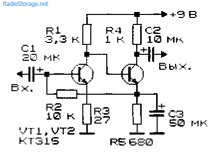
Rice. 13. Two-stage low-frequency amplifier using KT315 transistors - option 2.
The microphone amplifier (Fig. 11) is characterized by a low level of self-noise and a high gain [MK 5/83-XIV]. An electrodynamic type microphone was used as the VM1 microphone.
A telephone capsule can also act as a microphone. Stabilization of the operating point (initial bias at the base of the input transistor) of the amplifiers in Fig. 11 - 13 is carried out due to the voltage drop across the emitter resistance of the second amplification stage.

Rice. 14. Two-stage ULF with field-effect transistor.
The amplifier (Fig. 14), which has a high input resistance (about 1 MOhm), is made on a field-effect transistor VT1 (source follower) and a bipolar transistor - VT2 (with a common one).
A cascade low-frequency amplifier using field-effect transistors, which also has a high input impedance, is shown in Fig. 15.

Rice. 15. circuit of a simple two-stage ULF using two field-effect transistors.
ULF circuits for working with low-Ohm loads
Typical ULFs, designed to operate with low-impedance loads and having an output power of tens of mW and higher, are shown in Fig. 16, 17.

Rice. 16. A simple ULF for working with a low-resistance load.
Electrodynamic head BA1 can be connected to the output of the amplifier, as shown in Fig. 16, or diagonally to the bridge (Fig. 17). If the power source is made of two series-connected batteries (accumulators), the right output of the head BA1 according to the diagram can be connected to their midpoint directly, without capacitors SZ, C4.

Rice. 17. Circuit of a low-frequency amplifier with the inclusion of a low-resistance load in the diagonal of the bridge.
If you need a circuit for a simple tube ULF, then such an amplifier can be assembled even using one tube, look at our electronics website in the corresponding section.
Literature: Shustov M.A. Practical circuit design (Book 1), 2003.
Corrections in the publication: in Fig. 16 and 17, instead of diode D9, a chain of diodes is installed.
HIGH QUALITY PRE-AMPLIFIER CIRCUIT
At the turn of 2004 and 2005, a natural desire arises to build amplifiers on a modern element base, taking advantage of the advanced achievements of global electronic technology.
I bring to your attention a high-quality preamplifier based on the EL2125.
The basic materials are FREE and DIYers are free to use them to replicate them in their own designs.
WHY EL2125?
An excellent chip, according to its characteristics it almost ranks 2nd in the top ten op amps according to model reviews in 2004.
This is, of course, not the AD8099 (first place in the world, award from Intel “Innovation of 2004”), but the EL2125 has already appeared on the CIS market and it is quite possible to get it, especially for those who live in capitals and large cities.
JUDGE FOR YOURSELF HOW GOOD THE EL2125'S CHARACTERISTICS ARE:
Ability to operate on loads up to - 500 Ohm
Operating frequency range up to - 180 MHz
Supply voltage - ±4.5 ... ±16.5 V.
Nonlinear distortion coefficient - less than 0.001%
Output slew rate - 190 V/µs
Noise level - 0.86 nV/vHz (better than AD8099!!!)
The EL2125 retail price is usually $3 each, not very cheap, but worth it.
Most often, EL2125 is found in SO-8 type housing (prepare micro-tips for soldering irons).
I should note that I would add “amazing musicality” to the list of characteristics. This indicator cannot be measured with instruments and expressed in numbers; it is felt only by ear.
1. As an amplifier for phones with a wide range of impedances:

2. As a high-quality preamplifier for power amplifiers with bipolar power supply (ranging from ± 22 to ± 35 V.) and sensitivity 20 ... 26 dB:

This op-amp involuntarily suggests itself as a more serious pre-amplifier, created on the basis of the Solntsev amplifier and described on the Soldering Iron website:
The amplifier uses dual variable resistors R11 and R17 of any type of group B, R1 and R21 of any type of group B or A. A 100 kOhm variable resistor (tapped from the middle) can be used as a loud-compensated volume control (R21). Transistors can be replaced with KT3107I, KT313B, KT361V,K (VT1, VT4) and KT312V, KT315V (others). Replacing the K574UD1 op amp with other types of op amp is not recommended. If the DC component is at a significant level (in rare cases) at point A, it is necessary to install a capacitor with a capacity of 2.2 - 5 μF.
The described preamplifier is connected to an AF power amplifier with an input impedance of at least 10 kOhm. With a significant increase in Kg, this control unit can also be loaded onto an UMZCH with Rin up to 2 kOhm (which is extremely undesirable), in such cases (if the Rin of your UMZCH is less than 10 kOhm), you just need to once again power up the output stage (a copy of the circuit section VT1-VT2- VT3-VT4-R4-R5-R6-R7, connect to output DA2), connect resistors R23 and R24 in the same way as resistors R2 and R3, although in this case the noise level may increase. And if Rin of your UMZCH is greater than or equal to 100 kOhm, then it is recommended to use K574UD1A(B) as an operational amplifier DA2, this will reduce the level of distortion and noise.
Possible changes in the scheme (improving):
- To exclude P2K switches (very unreliable in operation) from the audio signal path, it is recommended to exclude switch SA1 from the circuit (together with resistors R8, R9), and move switch SA2 to the last stage by short-circuiting resistor R23 (resistors R13, R14 are excluded in this case from the diagram).
Preamp circuit:

It would also not be useless to use this op-amp in a universal pre-amplifier that can also serve as a headphone amplifier. The circuit diagram is shown below:

Emitter followers VT1-VT2 unload the output of the op-amp, and then follows a circuit with local feedback, which further reduces non-linear distortions. Resistors R19 and R20 set the quiescent current of the window stage of the preamplifier, similar to power amplifiers, within 7-12 mA. In this regard, the last stage must be installed on a small heat sink
The page was prepared based on materials from the site http://yooree.narod.ru and http://cxem.net
Modern digital sources sound (CD players, DACs, etc.) have a very low noise level. Much lower than vinyl or magnetic tape. Because of this, the noise requirements of the subsequent amplification path today have become much higher than in the era of analog audio. In light of these requirements, the preamplifier described below was designed with the primary goal of achieving high-quality sound at ultra-low noise levels without the use of exotic or expensive components.
In most stages the author used his favorite operational amplifiers NE5532, but in some nodes they are used LM4562, since recently they have become more accessible and allow you to get much less distortion when operating with a low-impedance load.
What kind of music lover (and even more so an audiophile) is without vinyl? It is for them that the preamplifier is equipped with two background correctors for different types of pickups. In addition, the design has tone control, visual level indicator And balanced outputs, which today has become almost a standard for high quality audio equipment.
The block diagram of the preamplifier is shown in the figure:

Click to enlarge
All modules are assembled on separate printed circuit boards, which simplifies their placement in the housing and facilitates switching.
This part of the series of articles describes the circuit of the amplifier itself with volume, balance and tone controls, as well as the organization of a symmetrical output.
Schematic diagram of the pre-amplifier module:

Click to enlarge
All resistances (not only resistors, but also the resistance of active components, for example the base resistance of a transistor) generate noises, the level of which depends on the resistance value and temperature. Since it is quite difficult to influence the temperature in the listening room, the only way to reduce the noise of the resistances is to reduce the value of the resistance itself. This implies the main feature of the presented scheme - the use low resistance resistors along the entire path of the sound signal.
If for constant resistors the choice of low-resistance ratings does not pose a problem, then for variable resistors (for volume, balance and tone controls) the nominal range is significantly limited. Typically in these circuits you can see variable resistors of 47 kOhm, 22 kOhm, or at best 10 kOhm. In this design, Douglas Self used 1kOhm variable resistors - this is perhaps the minimum value available among variable resistors.
By the way, here are the characteristics that we managed to achieve:
(Measurements were carried out at a supply voltage of 17V, with tone controls disabled, using balanced inputs and outputs)
| Harmonic distortion + noise (input signal 0.2V, output signal - 1V) | 0.0015% (1 kHz, B = 22 Hz to 22 kHz) 0.0028% (20 kHz, B = 22 Hz to 80 kHz) |
| Harmonic distortion + noise (input signal 2V, output signal - 1V) | 0.0003% (1 kHz, B = 22 Hz to 22 kHz) 0.0009% (20 kHz, B = 22 Hz to 80 kHz) |
| Signal-to-noise ratio (at 0.2V input signal) | 96 dB (B = 22 Hz to 22 kHz) 98.7 dBA |
| Reproducible frequency band: | 0.2 Hz to 300 kHz |
| Maximum output signal level (at 0.2V input): 1.3V | |
| Balance adjustment | +3.6 dB to -6.3 dB |
| Bass adjustment | ±8 dB (100 Hz) |
| Treble adjustment | ±8.5 dB (10 kHz) |
| Channel separation (R->L) | -98 dB (1 kHz) -74 dB (20 kHz) |
| Channel separation (L->R) | -102 dB (1 kHz) -80 dB (20 kHz) |
Using low resistance resistors also reduces offset operational amplifiers input currents, which also reduces noise caused by fluctuations in op-amp currents.
To reduce the noise of active components, a parallel connection is used in the circuit cascades. Of course, one could use modern low-noise op-amps like AD797. But this will be much more expensive and more complicated (since one package contains only one op-amp). Please note that this is not about parallel connection microcircuits (when they are soldered on top of each other), but about the parallel connection of amplifier stages. Only in this case, the noise of the amplifying elements will be uncorrelated, due to which the overall noise level is reduced by 3 dB when 2 stages are parallelized. When 4 stages are connected in parallel, the noise decreases by 6 dB, i.e. twice.
If 8 cascades are parallelized, the noise will decrease by 9 dB, but for such a gain the costs are unreasonably high.
Due to the use of low-resistance resistors in the tone control, the capacitor values were much larger than usual. But today this is not a problem for modern element base.
Line input and balance control.
To reduce noise and interference, a filter R1C1 and R2C2 is installed directly at the amplifier input. Buffer stages IC1A and IC1B provide approximately 50kΩ input impedance and improve common mode rejection. The amplification stage itself is assembled on LM4562 (IC2A), the gain of which is adjusted by potentiometer P1A. The same potentiometer in the right channel is turned on “out of phase” with the left one, due to which the balance is adjusted. Feedback in the cascade it is implemented through two parallel buffers IC3A and IC3b, due to which the cascade gain remains constant regardless of load changes. In addition, this solution reduces noise and provides low output impedance.
A typical implementation of a balance control usually negatively affects the stage and the “virtual” arrangement of instruments, which is why it is quite rare in Hi-End equipment. Douglas Self's solution to this node does not have this drawback.
The noise level of this part of the preamplifier is only -109 dB in the middle position of the balance control, -106 dB at the maximum and -116 dB at the minimum position of the control (in the frequency band 22 Hz to 22 kHz).
Tone control.
Despite the fact that the regulator looks somewhat unusual, nevertheless, the classic Baxandall tone control circuit is used here. As noted above, due to the low denominations variable resistances The capacitor ratings are significantly higher than the “typical” values.
Capacitor C7 (1 μF) determines the lower tone control frequency, and capacitors C8 and C9 have a value of 100 nF and determine the tone control frequency at HF. If desired, the depth of tone control can be increased to ± 10 dB. Due to the IC4 elements, the mutual influence of the low-frequency and high-frequency circuits when controlling timbres is eliminated.
Despite the large dimensions and high cost, the use of polypropylene capacitors.
The tone control noise level is only -113 dB in the middle position of the controls.
Relay RE1 serves to turn off the tone control if it is not needed. In this case, the signal is taken from the output of IC2A and goes directly to the input of IC9B, bypassing the tone control. To avoid clicks during switching, resistor R18 is used. To reduce crosstalk, switching in each channel is carried out by a separate relay. In this case contact groups the relay can be parallelized, which will reduce the contact resistance and further increase the reliability of this part of the circuit.
Active volume control.
The volume control was also implemented according to the idea of Peter Baxandall, which firstly made it possible to obtain ultra-low noise level(especially at low volumes), and secondly, to obtain a logarithmic regulation characteristic when using potentiometers with linear dependence resistance depending on the angle of rotation. The maximum gain is +16 dB, with the 0 dB point obtained at the middle position of the potentiometer.
Four amplifiers connected in parallel, as noted above, serve to reduce the noise level by 6 dB. The self-noise level of such a regulator is -101 dB at maximum gain and -109 dB at 0 dB gain. In practice, the volume control is usually set to -20 dB, then the noise level will be -115 dB, which is significantly below the hearing threshold.
So that you can evaluate the quality of each cascade, their own noise levels are given. The resulting noise level of a given preamplifier, as you might guess, will vary somewhat depending on the position of the potentiometers.
Symmetrical output implemented using a phase inverter on the op-amp IC9A and has double the signal amplitude compared to an asymmetrical one. However, this is normal for professional audio equipment.
Design and setup.
Placement of amplifier elements on the board:

Click to enlarge
During assembly, the resistors are soldered first, and then the remaining components.
Jumper JP1 is designed to select optimal connection vinyl corrector ground (there are similar jumpers on MC / MD boards). Don't forget to connect them. The connection location is selected experimentally after assembling the structure in the housing.
Photo of the assembled board:

Click to enlarge
This block of settings does not require.
Frequency characteristics of the amplifier and tone control:

Click to enlarge
List of elements:
Resistors:
(1% accuracy; metal-film; 0.25W)
R1,R2,R39,R40 = 100Ohm
R3-R6,R41-R44,R78,R79 = 100kOhm
R7-R12,R16,R17,R21-R24,R33,R34,
R45-R50,R54,R55,R59-R62,R71,R72 = 1kOhm
R13,R51 = 470Ohm
R14,R15,R52,R53 = 430Ohm
R18,R35,R36,R56,R73,R74 = 22kOhm
R19,R20,R57,R58 = 20Ohm
R25-R28,R63-R66 = 3.3kOhm
R29-R32,R67-R70 = 10Ohm
R37,R38,R75,R76 = 47Ohm
R77 = 120Ohm
P1,P2,P3,P4 = 1kOhm, 10%, 1W, stereo potentiometer, linear, for example Vishay Spectrol cermet type 14920F0GJSX13102KA. or, Vishay Spectrol conductive plastic type 148DXG56S102SP.
Capacitors:
C1,C2,C10-C14,C26,C27,C35-C39 = 100pF 630V, 1%, polystyrene, axial
C3,C4,C28,C29 = 47µF 35V, 20%, non-polar, 8mm diameter, 3.5mm pin spacing, e.g. Multicomp p/n NP35V476M8X11.5
C5,C6,C30,C31 = 470pF 630V, 1%, polystyrene, axial
C7,C32 = 1µF 250V, 5%, polypropylene, pin spacing 15mm
C8,C9,C33,C34 = 100nF 250V, 5%, polypropylene, lead spacing 10mm
C15,C16,C40,C41 = 220µF 35V, 20%, non-polar, 13mm diameter, 5mm pin spacing, e.g. Multicomp p/n NP35V227M13X20
C17-C25,C42-C50 = 100nF 100V, 10%, pin spacing 7.5mm
C51 = 470nF 100V, 10%, pin spacing 7.5mm
C52,C53 = 100µF 25V, 20%, diameter 6.3mm, pin spacing 2.5mm
Chips:
IC1,IC3,IC5-IC10,IC12,IC14-IC18 = NE5532, for example ON Semiconductor type NE5532ANG
IC2,IC4,IC11,IC13 = LM4562, for example National Semiconductor type LM4562NA/NOPB
Miscellaneous:
K1-K4 = 4-pin connector, pitch 0.1’’ (2.54mm)
K5,K6,K7 = 2-pin connector, pitch 0.1’’ (2.54mm)
JP1 = 2-pin jumper, pitch 0.1’’ (2.54mm)
K8 = 3-pin screw block, 5mm pitch
RE1,RE2 = relay, 12V/960Ohm, 230VAC/3A, DPDT, TE Connectivity/Axicom type V23105-A5003-A201
To be continued...
The article was prepared based on materials from the magazine “Elector” (Germany)
Happy creativity!
Editor-in-Chief of RadioGazeta


