A set for studying the operation of logical elements. Research of logical elements and synthesis of logic circuits Report on the study of logical elements
1. Purpose of the work
The purpose of the work is:
Theoretical study of logical elements that implement elementary functions of logic algebra (FAL);
Experimental study of logic elements built on domestic K155 series microcircuits.
2. Basic theoretical principles.
2.1. The mathematical basis of digital electronics and computer technology is the algebra of logic or Boolean algebra (named after the English mathematician John Bull).
In Boolean algebra, independent variables or arguments (X) take only two values: 0 or 1. Dependent variables or functions (Y) can also take only one of two values: 0 or 1. A logic algebra function (FAL) is represented as:
Y = F (X 1; X 2; X 3 ... X N).
This form of specifying FAL is called algebraic.
2.2. The main logical functions are:
Logical negation (inversion)
Logical addition (disjunction)
Y = X 1 + X 2 or Y = X 1 V X 2 ;
Logical multiplication (conjunction)
Y = X 1 X 2 or Y = X 1 L X 2.
More complex logical algebra functions include:
Equivalence function
Y = X 1 · X 2 + or Y = X 1 ~ X 2 ;
Disparity function (addition modulo two)
Y = X 1 · + · X 2 or Y = X 1 X 2 ;
Pierce function (logical addition with negation)
Schaeffer function (logical multiplication with negation)
2.3. The following laws and rules apply to Boolean algebra:
Distributive law
X 1 (X 2 + X 3) = X 1 X 2 + X 1 X 3,
X 1 + X 2 · X 3 = (X 1 + X 2) (X 1 + X 3) ;
Repetition rule
X · X = X, X + X = X;
Negation rule
X = 0, X + = 1;
De Morgan's theorem
Identities
X 1 = X, X + 0 = X, X 0 = 0, X + 1 = 1.
2.4. Circuits that implement logical functions are called logical elements. Basic logical elements, as a rule, have one output (Y) and several inputs, the number of which is equal to the number of arguments (X 1 ; X 2 ; X 3 ... X N). On electrical diagrams, logic elements are designated as rectangles with pins for input (left) and output (right) variables. Inside the rectangle is a symbol indicating the functional purpose of the element.
Figure 1 ¸ 10 shows the logical elements that implement those discussed in clause 2.2. functions. The so-called state tables or truth tables are also presented there, describing the corresponding logical functions in binary code in the form of states of input and output variables. The truth table is also a tabular way of specifying FAL.
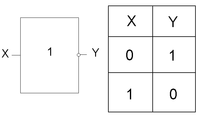
Figure 1 shows the “NOT” element that implements the logical negation function Y = .
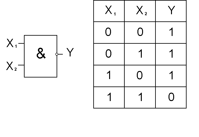
The “OR” element (Fig. 2) and the “AND” element (Fig. 3) implement the functions of logical addition and logical multiplication, respectively.


Peirce functions and Schaeffer functions are implemented using the “OR-NOT” and “AND-NOT” elements presented in Fig. 4 and Fig. 5 respectively.

The Peirce element can be represented as a sequential connection of an “OR” element and a “NOT” element (Fig. 6), and the Schaeffer element can be represented as a sequential connection of an “AND” element and a “NOT” element (Fig. 7).

Figure 8 and Figure 9 show the elements “Exclusive OR” and “Exclusive OR - NOT”, which implement the functions of disparity and disparity with negation, respectively.


2.5. Logical elements that implement the operations of conjunction, disjunction, Peirce and Schaeffer functions can, in the general case, be n-input. For example, a logic element with three inputs that implements the Pierce function has the form shown in Fig. 10.
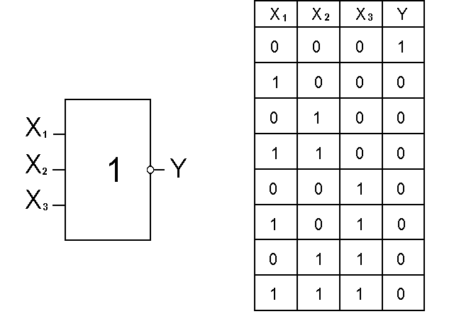
In the truth table (Fig. 10), unlike the tables in clause 2.4. there are eight values of the output variable Y. This number is determined by the number of possible combinations of input variables N, which, in general, is equal to: N = 2 n, where n is the number of input variables.
2.6. Logic elements are used to build integrated circuits that perform various logical and arithmetic operations and have various functional purposes. Microcircuits of the K155LN1 and K155LA3 types, for example, contain six inverters and four Schaeffer elements, respectively (Fig. 11), and the K155LR1 microcircuit contains elements of different types (Fig. 12).


2.7. FAL of any complexity can be implemented using the specified logical elements. As an example, consider the FAL, given in algebraic form, in the form:
Let's simplify this FAL using the above rules. We get:
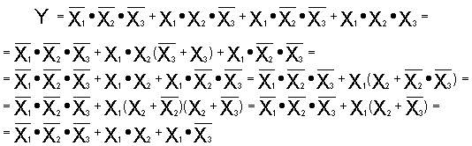 (2)
(2)
The operation performed is called FAL minimization and serves to facilitate the procedure for constructing a functional diagram of the corresponding digital device.
The functional diagram of the device that implements the FAL under consideration is presented in Fig. 13.

It should be noted that the function (2) obtained after transformations is not completely minimized. Complete minimization of the function is carried out during laboratory work.
3. Description of the object and research tools
The device studied in laboratory work is shown in Fig. 14.
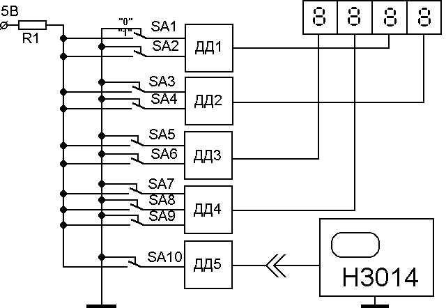
3.1. The device is a group of logical elements made on K155 series microcircuits (elements DD1-DD4).
For microcircuits of this series, a logical unit corresponds to a voltage U 1 = (2.4 ¸ 5.0) V, and a logical zero - U 0 = (0 ¸ 0.8) V.
3.2. Logical “0” and “1” at the input of the elements are set using the buttons located on the front panel of the K32 block under the inscription “Code programmer”. The button numbers on the panel correspond to the numbers on the device diagram.
A complete graphical representation of buttons of this type (so-called “latching buttons”) is shown only for button SA1.
When the button is pressed, the input of the elements is connected through resistor R1 to a source with a voltage of 5V. In this case, voltage U 1 will act at the input of the elements, which corresponds to the supply of a logical unit to the output of the microcircuit. When the button is pressed, the input of the element will be connected to a bus located at ground potential, which corresponds to applying a logical zero U 0 to the output of the microcircuit.
3.3. Logical signals from the terminals of elements DD1 ¸ DD4 are supplied to digital indicators and are induced in the form of symbols “0” and “1”. Digital indicators are located in the K32 block on the left (“IO 2” button) under the indicators must be pressed.
3.4. The signal from the output of the DD5 element is fed through the switching circuit to the input of the H3014 multimeter. First, the multimeter is set to the “-V” DC voltage measurement mode and the following connections are made:
3.4.1. The input - the multimeter socket “-V” - is connected with a cable to the “Output V ~“ socket of the K32 block.
3.4.2. The XS1 socket on the device board is connected by a conductor to the left socket under the “Input 1” inscription in the “Switch” inscription field.
3.4.3. The “VSV VNK” button above the above socket must be pressed.
3.4.4. The “VX 1” button under the inscription “Control V ~“ should be pressed, and the “VSV VNK” button in the “KVU” inscription field should be in the released state.
4.1. Study of the functioning features of logical elements DD1 ¸ DD4 and determination of their functional purpose.
4.1.1. By specifying various combinations of input logical signals, determine the value of the output signal and, based on the measurement results, fill out the truth tables for each element DD1 ¸ DD4 (Table 1 or Table 2, respectively) in the laboratory report.
Table 1.
Table 2.
4.1.2. Based on the measurement results (clause 4.1.1.), determine the functional purpose of the elements and indicate their designation on the diagram in the laboratory report.
Attention! It is strictly prohibited to introduce designations into the text of methodological instructions.
4.2. Study of the functioning features of the DD5 element, determination of its functional purpose and measurement of voltage levels corresponding to the logical signals “0” and “1”.
4.2.1. By setting the logical signals “0” and “1” using the SA12 button, determine its functional purpose at the input of the DD5 element based on the ratio of the output signals (see section 3.1.). Measure the voltage value at the output of the element for each combination of input signals using a multimeter (section 3.4.). Enter the measurement data into the table.
Table 3.
4.2.2. Based on the measurement results (clause 4.2.1.), determine the voltage levels of logical zero U 0 and logical one U 1 for a given type of microcircuit and establish their compliance with the passport data.
4.3. Carry out complete minimization of the FAL presented in paragraph 2.7. Based on the results of minimization, draw up a functional diagram of the device.
1. Title and purpose of the work
2. Diagram of the device under study
3. Tables 1,2,3
4. Results of measurements of U 0 and U 1 (clause 4.2.2.)
5. Formulas for calculation and calculation according to clause 4.3., device diagram
6. Conclusions from the work
6. Security questions
1. What values of variables does the algebra of logic operate on?
2. Basic forms of FAL assignment
3. Type of basic logical functions in algebraic form
4. What is a “logical element”?
5. What logical functions do Peirce and Schaeffer elements perform?
6. What determines the number of possible combinations of input variables for an arbitrary logical element?
7. List of references
Electrical engineering and fundamentals of electronics. O.A.Antonova, O.P.Gludkin and others, ed. prof. O.P.Gludkina.-M.: Higher School, 1993.
Laboratory work No. 2
1. PURPOSE OF THE WORK
Study of the functioning of typical logical elements; implementation of basic and other functions using basic AND-NOT and OR-NOT elements; the use of logical elements as signal switches.
2. THEORETICAL PROVISIONS
ICs of the LA type perform the logical function mAND - NOT, ICs of the LE type perform the logical function mOR - NOT (m is the number of inputs), and ICs of the LN type perform the logical function NOT. One package of the LAZ microcircuit contains four 2I-NOT logic elements. One package of the LE1 microcircuit contains four 2OR-NOT logic elements. One package of the LN1 microcircuit contains six logical NOT elements (inverters). The LN1 microcircuit has a push-pull output stage. The symbols and pinouts of the LAZ, LE1 and LN1 microcircuits are shown in Fig. 1.
Picture 1
Logic elements are also called gates (signal switches). This is because they can delay or allow digital information to pass through, much like a valve designed to control the flow of fluid. The symbol for the 2I valve with the signals at its inputs and output and the timing diagrams of its operation as a switch are shown in Fig. 2.

Figure 2
If rectangular pulses from the generator are applied to the upper input of the 2I logical element, and a logical unit level is applied to the lower input, then the pulses from the generator will pass to the output of the 2I logical element (Fig. 2). This follows from the law of operation of the AND element. If the logical one at the lower input is replaced by a logical zero, then pulses from the upper input to the output of the logical element 2I will not pass, since at least one zero at the input of this element gives a zero at the output.
3. EQUIPMENT
The TsS-02 stand is used as measuring equipment.
4. PROCEDURE FOR PERFORMANCE OF THE WORK
In your work, use the K155JIA3, K155LE1, K155LN1 microcircuits.
1. Study of the functioning of logical elements 2AND-NOT, 2OR-NOT and NOT
1.1. Draw diagrams for studying logical elements (see Fig. 3 a - c). Put on them the numbers of the pins of the selected elements of the microcircuits. Select the LU sources that you will use and put their numbers on the diagram.
1.2. Assemble the circuits shown in these figures one by one.
1.3. By changing combinations of input signals, monitor the output state of the logic element under study with an LED indicator or an oscilloscope. Fill in the truth tables of the elements (Table 1).
Table 1
| A | IN | LA3 | LE1 | LN1 |
| Function |
1.4. Make sure the logic elements are functioning correctly.

Figure 3
2. Implementation of basic functions on basic NAND elements
2.1. Draw the diagrams shown in Fig. 4,a, 4,c. Put on them the numbers of the pins of the selected elements of the microcircuits. Select the LU sources that you will use and put their numbers on the diagram.
 Figure 4
2.2.Assemble the circuits shown in these figures one by one.
2.3.When changing combinations of input signals, monitor the state of the outputs of all logical elements of the circuits with LED indicators or an oscilloscope. Create truth tables for the circuits under study.
2.4. Make sure that the results obtained are correct by theoretically analyzing the operation of the circuits under study.
2.5.Using the obtained truth tables, determine the type of function that each circuit performs and write the name of the function in the “type of function” column of the tables.
3. Implementation of basic functions on basic OR-NOT elements
3.1. Draw the diagrams shown in Fig. 5, a, b, c. Put on them the numbers of the pins of the selected elements of the microcircuits. Select the LU sources that you will use and put their numbers on the diagram.
 Figure 5.
3.2. Assemble the circuits shown in these figures one by one.
3.3. By changing combinations of input signals, monitor the state of the outputs of all logical elements of the circuits with LED indicators or an oscilloscope. Fill in the truth tables of the circuits under study, similar to the table. 3...5.
3.4. Make sure the results obtained are correct by theoretically analyzing the operation of the circuits under study.
3.5. Using truth tables, determine the type of function that each circuit performs and write the name of the function in the “type of function” column of the tables.
4. Implementation of functions of various types on basic elements AND-NOT and OR-NOT
4.1. Draw the diagrams shown in Fig. 6, a, b. Put on them the numbers of the pins of the selected elements of the microcircuits. Select the LU sources that you will use and put their numbers on the diagram.

Figure 6
4.2. Assemble the circuits shown in these figures one by one.
4.3. By changing combinations of input signals, monitor the state of the outputs of all logical elements of the circuits with LED indicators or an oscilloscope. Fill in the truth tables of the circuits under study.
4.4. Make sure the results obtained are correct by theoretically analyzing the operation of the circuits under study.
5. Application of logic elements as signal switches
5.1. Draw circuits for studying logical elements (see Fig. 7, a - d). Put on them the numbers of the pins of the logical elements of the microcircuits selected for research. Select the LU sources that you will use and put their numbers on the diagram.
5.2. Assemble one by one the circuits shown in Fig. 7, a, c, if there are only LED indicators to control input and output signals. If you have an oscilloscope, assemble the circuits shown in Fig. 7, c, d.
5.3. Observe the waveform at input A of the logic gates and output signal C, first when there is a logical one at input B, and then when there is a logical zero. To do this, connect an LED indicator to the output of the circuits (Fig. 7, a, c). When studying circuits (Fig. 7, c, d), connect the input of the first channel of the oscilloscope to the input A of the logical element, and the input of the second channel to the output of the logical element. Synchronize the oscilloscope sweep with the signal of the first channel. Draw timing diagrams (oscillograms) of the signals at the inputs and outputs of the elements under study for both cases (Fig. 8 a, b).
5.4. Verify the correct functioning of logic elements as signal switches by theoretically analyzing their operation.

Figure 7

Figure 8
The work report must contain:
Title of the work and purpose of the work;
Schemes under study;
Truth tables;
Timing diagrams;
Comparison of experimental data with the results of theoretical analysis;
Conclusions from the work.
CONTROL QUESTIONS
1. How many different combinations are there for the four input signals?
2. What does the symbol for the ZILI logical element look like?
3. How will the output function of a NAND gate change if its inputs are inverted?
4. Which logic gates invert input signals when passing them to the output?
5. What signals must be supplied to the other two inputs of the ZILI logic element so that pulses from the first input pass to the output?
E.N. Malysheva
Basics
Microelectronics
Laboratory workshop
Tobolsk - 2012
UDC 621.3.049.77
Published by decision of the Department of Technology and Technical Disciplines of the TSPI named after. DI. Mendeleev
Malysheva E.N. Fundamentals of microelectronics. Laboratory workshop: Textbook. – Tobolsk: TGPI named after. DI. Mendeleeva, 2012. – 60 p.
Reviewer: Novoselov V.I., Ph.D. Sc., Associate Professor, Department of Physics and MPF
© Malysheva E.N., 2012
© TGPI named after. DI. Mendeleev, 2012
Explanatory note
This textbook is made in the form of a workbook and is offered to accompany a laboratory workshop for students of pedagogical universities studying the fundamentals of microelectronics. The laboratory workshop is conducted using a universal stand and is devoted to the study of elements, components and devices of digital technology.
1. Study of the operation of basic logical elements.
2. Study of the operation of triggers.
3. Study of the operation of registers.
4. Study of the operation of combinational code converters.
5. Study of the operation of meters.
6. Study of the operation of the adder.
7. Study of the operation of an arithmetic-logical device.
8. Study of the operation of a random access memory device.
9. Study of the operation of a computer model.
Each work includes the following sections:
Theoretical material, the mastery of which is necessary to complete the work;
Description of work;
Questions for the test of this work.
Laboratory work No. 1.
Study of the operation of basic logical elements
Goal of the work: study of operating principles and experimental study of the operation of logical elements.
General information
Logical elements, together with storage elements, form the basis of computers, digital measuring instruments and automation devices. Logic elements perform the simplest logical operations on digital information. They are created on the basis of electronic devices operating in key mode, which is characterized by two key states: “On” - “Disabled”. Therefore, digital information is usually represented in binary form, when the signals take only two values: “0” (logical zero) and “1” (logical one), corresponding to the two states of the key. These two positions (logical 1 and logical 0) constitute the electronic alphabet, or the basis of binary code.
The input of any digital device receives a set of code words, which it converts into other code words or a word. The output codewords are a certain function for which the input codewords are the argument of this function. They are called logical algebra functions.
Logical functions, like mathematical ones, can be written in the form of a formula or table - a truth table, which lists all possible combinations of arguments and the corresponding values of logical functions. A device designed to perform certain functions of the algebra of logic is called a logical element. Let's look at some of them.
Logic element NOT
logical negation (inversion). The logical negation of a statement A is a statement X that is true when A is false..


Logic element AND
Designed to perform a function logical multiplication (conjunction).Logical multiplication is a connection between two simple statements A and B, as a result of which a complex statement X is true only if both statements are true at the same time.


Logic element AND-NOT
Designed to perform a function negation of logical multiplication (negation of conjunction).The negation of multiplication or the Schaeffer function is a connection between two simple statements A and B, as a result of which a complex statement X is false only if both statements are true at the same time.

![]()
Work order
Equipment: universal stand, power supply, P1 board, technological cards I-1 - I-9.
1. Analyze the operation of the LED indicator of the stand to determine the levels of logical signals.
2. Examine the operation of logical devices, sequentially using technological maps. Complete the following tasks for each diagram:
A. fill in the truth tables,
b. using the data obtained, identify the logical elements,
V. name the logical algebra functions they perform,
d. designate the logical elements on the diagram with the corresponding symbols,
d. write down formulas expressing the relationship between input and output characteristics.
 |
Questions for testing 1. What is the purpose and scope of logical elements? 2. Define basic logical functions. 3. Using the LED indicator, determine the level of the logic signal at the output of the circuit. 4. Determine the types of logical elements in the circuit from the output data. 5. Based on the markings of integrated circuits located on the board used, give their characteristics. Laboratory work No. 2. General information More complex digital devices are built from logic elements. One of the most common components of digital technology is the trigger. A trigger is a device that has two stable equilibrium states and is capable of jumping from one state to another under the influence of a control signal. Each trigger state corresponds to a certain (high or low) output voltage level, which can be maintained for any length of time. Therefore, triggers are called the simplest digital automata with memory, i.e. their state is determined not only by the input signals at a given time, but also by their sequence in the previous clock cycles of the trigger. Currently, most flip-flops are based on logic elements in the form of integrated circuits (ICs). They are used as switching elements independently or as part of more complex digital devices, such as counters, frequency dividers, registers, etc. Based on the method of recording information, triggers are divided into synchronous and asynchronous devices. In asynchronous triggers, information is recorded directly with the arrival of input signals. In synchronous (clock) flip-flops, information will be recorded only if there is a clock sync pulse. According to their functional characteristics, triggers are distinguished: with separate triggering (RS-triggers), with delay elements (D-triggers), with counting triggering (T-triggers), universal (JK-triggers). Typically, a trigger has two outputs: forward () and inverse (). The state of the trigger is determined by the voltage at the direct output. Trigger inputs have the following designations: S – separate input for setting the trigger to a single state; R – separate input for setting the trigger to the zero state; D – information input; C – synchronization input; T – counting input and others. The basis of all flip-flop circuits is an asynchronous RS flip-flop. There are two types of RS flip-flops: those built on logical elements “OR-NOT” and those built on logical elements “AND-NOT”. They differ in the level of active signals and have their own designation (see table). RS flip-flops have operating modes: setting to zero or one state, storage, prohibited mode. A forbidden combination (active signals are supplied to both inputs) is implemented when a contradictory command is given: simultaneously set to one and zero states. In this case, the same voltage levels are realized at the direct and inverse outputs, which by definition should not be the case. Clocked D-flip-flops have an input D for supplying information (0 or 1) and a clock input C. Synchronization pulses (C = 1) from a special pulse generator are supplied to input C. D flip-flops are free of prohibited combinations of input signals. A counting T flip-flop has one control input T. The trigger states change whenever the control signal changes. T-flip-flops of one type react to the front of a pulse, i.e. for a difference of 0-1, others - for a cut (difference of 1-0). In any case, the frequency of the output pulses is 2 times lower than the frequency of the input pulses. Therefore, T-triggers are used as frequency dividers by 2 or modulo 2 counters. Triggers of this type are not available as ICs. They can be easily created based on D and JK flip-flops. JK flip-flops are universal, they have information inputs J and K and a synchronizing input C. They are used to create counters, registers and other devices. With certain input switching, JK flip-flops can work as RS flip-flops, D flip-flops and T flip-flops. Due to this versatility, they are available in all IC series. Work order Equipment: universal stand, power supply, P2 board, technological cards II-1 - II-4. 1. Select a trigger in the circuit. 2. Complete the following tasks for each diagram: a) write down the name of the trigger, b) make a table of state changes depending on the input signals, indicate active signals with an arrow ( - high level - logical one, ¯ - low level - logical zero), c) determine the type of input (R or S), indicate these designations in the table and indicate on the diagram (for cards II-1 and II-2), d) indicate the operating modes of the trigger, e) draw up a time diagram of trigger states.
Trigger ______________________________________________________________
Trigger ______________________________________________________________
Trigger ______________________________________________________________
Questions for testing 1. What is a trigger? 2. Explain the purpose of flip-flop inputs. 3. What is active signal level? 4. What is the difference between synchronous and asynchronous triggers? 5. Explain the nature of the “forbidden” state in an RS flip-flop. 6. Using the diagram, tell us about the state of the trigger at each cycle of operation. 7. Based on the markings of integrated circuits located on the board used, give their characteristics. Laboratory work No. 3. General information A register is an operational unit consisting of flip-flops and designed to receive and store information in binary code. The length of the codewords written to the register depends on the number of trigger cells that make it up. Because a trigger can only assume one stable state at a given time, then, for example, to write a 4-bit word, you must have a register of four trigger cells. Based on the method of writing code words, parallel, sequential (shifting) and universal registers are distinguished. In parallel registers, the codeword is written in parallel form, i.e. to all trigger cells simultaneously. In a serial register, the codeword is written sequentially, starting from the least significant or most significant digit. All flip-flops included in the register are united by a common synchronization input; some types of circuits have a common input R for the zeroing operation.
Work order Equipment: universal stand, power supply, boards P2, P3, jumper, technological cards II-5, II-6, III-1, III-2. 1. Write down the name of the device indicating its bit capacity. 2. Analyze the operation of two-bit registers. 3. Complete the following tasks for each diagram: a) write down the name of the register, b) write several different code words into the register, enter the results into a table of dependences of output states on input signals, c) draw a symbol for the device, II-5 (P2) |


II-6 (P2)
_______________________________________________________________

Conclusion: ________________________________________________________
________________________________________________________
4. For four-bit registers, complete the tasks:
a) write down the name of the register indicating its capacity,
b) sketch the internal logical structure,
c) write several different code words into the register, enter the results into a table of dependences of output states on input signals,
d) draw a conclusion: how many clock cycles does it take to write one code word in this register?
III-1 (P3)
_______________________________________________________________

| Entrance | Exits | |||
| D | Q4 | Q3 | Q2 | Q1 |
 |
| Entrance | Exits | |||
| D | Q4 | Q3 | Q2 | Q1 |
Conclusion: _________________________________________________________
_________________________________________________________
III-2 (P3)
_______________________________________________________________

| Inputs | Exits | ||||||
| D4 | D3 | D2 | D1 | Q4 | Q3 | Q2 | Q1 |

Conclusion: ___________________________
___________________________
Questions for testing
1. What device is called a register? What is it for?
2. What types of registers do you know? How are they different?
3. Explain the concept of “bit depth”. What does the expression "4-bit register" mean?
4. How do you need to change the functional diagram to get a four-bit register from a two-bit register?
5. How many different words can be written using a 2 (4) bit register?
6. Explain on each functional diagram how you recorded the code word?
Laboratory work No. 4.
General information
Combinational code converters are designed to convert an m-element parallel code at the inputs of a digital machine into an n-element code at its outputs, i.e. to convert a codeword from one form to another. The relationship between input and output data can be specified using logical functions or truth tables. The most common types of code converters are encryptors, decryptors, multiplexers, and demultiplexers.
Encoders are used in information input systems to convert a single signal at one of its inputs into a multi-bit binary code at the outputs. Thus, the signal from each key on the keyboard, indicating a number or letter, is sent to the corresponding input of the encoder, and at its output this symbol is displayed in a binary code word. Decoders perform the reverse operation and are used in information output systems. To visually evaluate the output information, decoders are used together with display systems. One type of indicator is the 7-segment LED or liquid crystal indicator. To do this, the output signals of the decoder are converted into the code of a 7-segment indicator.
Multiplexers solve the problem of selecting information from several sources, demultiplexers solve the problem of distributing information among several receivers. These devices are used in digital technology processor systems to connect individual processor units with each other.
Work order
Equipment: universal stand, power supply, P4 board, technological cards IV-1, IV-2, IV-3.
1. Analyze the operation of the decoder.
2. Complete the following tasks for schemes IV-1 and IV-2:
a) make a table of the dependence of output states on input signals,
b) draw a conclusion: from which coding system does the device translate to which?
c) how many digits does a binary number have in circuit IV-2? What task does the SA5 toggle switch perform?
Multiplexer
3. Analyze the operation of a circuit containing a multiplexer and complete the tasks:
a) find the multiplexer in the diagram,
b) check where the information comes from at the multiplexer inputs,
c) check what device is used to set the address to the multiplexer,
d) set the multiplexer the address of the information input from which you want to send the signal to its output,
e) fill out the table of the dependence of the output signal on the input information and the address given to the multiplexer, entering different addresses and supplying different information to the inputs.

| Address | No. D-input connected to the output | Input information | Output Y | |||||||||
| A2 | A1 | A0 | D0 | D1 | D2 | D3 | D4 | D5 | D6 | D7 | ||
Questions for testing
1. What device is called a decoder? What is it for?
2. What device is called a multiplexer? What is it for?
3. What type of indication is used in scheme IV-2?
4. What does the expression “binary information coding system” (decimal, hexadecimal) mean?
Goal of the work: 1) studying the principles of constructing serial logic chips;
2) study of logical functions of one and two variables and their implementation.
General information:
Logic elements(LE) are widely used in automation, computer technology and digital measuring instruments. They are created on the basis of electronic devices operating in a key mode, in which signal levels can take only two values. In positive logic, it is accepted that a high signal level corresponds to a logical one (1), and a low signal level corresponds to a logical zero (0).
A logical function expresses the dependence of output logical variables on input ones and takes the values 0 or 1. It is convenient to represent any logical function in the form of a state table (truth table), where possible combinations of arguments and the corresponding functions are written.
The operation of logic devices is analyzed using logic algebra (Boolean algebra), where a variable can take only two values: 0 or 1.
The main logical operations are (Table 1):
1) logical multiplication: y=x 1 · x 2 ·...· x n (read “and X 1, and X 2 ,..., and X n");
2) logical addition: y=x 1 +x 2 +...+x n (read “or X 1, or X 2 ,..., or X n");
3) logical negation: (read “not X”).
As can be seen from Table 1, the output signal of the OR element is equal to 1 if at least one of its inputs is supplied with a 1 signal. The AND element produces 1 if all inputs are supplied with 1 signals.
All possible logical functions of n variables can be formed using a combination of three basic operations: AND, OR, NOT. Therefore, such a set is called a logical basis or functionally complete. Using the laws of Boolean algebra (Table 1), it is possible to prove that such are sets of one AND-NOT, OR-NOT function.
The basic elements of the same series use the same microcircuit implementation. The series is characterized by general electrical, design and technological parameters.
The 155 series integrated circuits are transistor-transistor logic (TTL) gates with 14 or 16 pins. The basic element of the series is the NAND logic element, consisting of a multi-emitter transistor VT1 and a complex amplifier-inverter.
Table 1
| Item Type | Logic function (operation) | Logical Operation Notation | Truth table | Conditional Image | ||||
| x 1 | ||||||||
| x 2 | ||||||||
| NOT element (inverter) | Logical Negation, Inversion | ù x | x | X 1y | ||||
| Element AND (conjunctor) | Logical multiplication, Conjunction | x 1 · x 2 x 1 x 2 x 1 Ù x 2 x 1 &x 2 | x 1 · x 2 | x 1 & y x 2 y=x 1× x 2 | ||||
| OR element (disjunctor) | Logical addition, disjunction | x 1 +x 2 x 1 Ú x 2 | x 1 +x 2 | x 1 1 y x 2 y=x 1 +x 2 | ||||
| NAND element (Schaeffer element) | Negation of conjunction | _____ x 1 · x 2 | _____ x 1 · x 2 | x 1 & y x 2 y= | ||||
| NOR element (Pierce element) | Negation of disjunction | _____ x 1 +x 2 | _____ x 1 +x 2 | x 1 1 y x 2 y= |
Currently, several types of series of microcircuits with TTL elements are used: standard (series 133; K155), high-speed (series 130; K131), micro-power (series 134). In addition to expanding the range of elements of the K531 and K555 series, the most promising TTLSh series are now being actively developed - micro-power K1533 and high-speed K1531, made on the basis of the latest achievements in IC manufacturing technology - ion implantation and precision photolithography.
 In recent years, programmable logic elements have developed, on which many digital devices can be built using programmers.
Any complex logical function can be implemented using LEs that perform the elementary functions AND-NOT, OR-NOT. Suppose you need to create a combinational circuit with four inputs x 1 , x 2 , x 3 , x 4 and one output y. A high voltage level should appear at the output only if there are high levels at three inputs, i.e. y=1 at x 1 =x 2 =x 3 =1 and x 4 =0. Such a scheme can be created by selecting elements. For example, the 3I-NOT element when applied to its inputs x 1 =x 2 =x 3 =1 gives the output signal y 1 =0. Serving it up and x 4 =0 to the input of the 2OR-NOT element, we get y=1 (Fig. 1).
Procedure for performing the experiment:
1) Install a block of logical elements (LE).
2) Connect the power supply GN1 to the “5V” sockets.
3) Study the operating principle of LE. To do this, apply signals (0 or 1) to their inputs. Monitor the outputs using a logic tester.
4) Assemble combinational circuits on the LE (Fig. 2).

 |
Check their work. Create truth tables for the circuits under study.
1. Job title.
2. Goal of the work.
3. Logic element circuits.
4. Truth tables.
5. Conclusion on the work.
In the output, indicate the purpose of the logical elements and their scope of application.
Control questions:
1. What operations of logical algebra do you know?
2. Give examples of the simplest digital devices based on logical elements.
3. Explain the operation of basic logic gates.
4. How LEs are classified according to their microcircuit implementation.
STUDY OF TRIGGERS ON LOGIC ICs.
Goal of the work: studying the circuits and functionality of the main types of triggers; experimental study of triggers and control circuits.
Laboratory work No. 2
Literature:
2. V.S. Yampolsky Fundamentals of automation and electronic devices. – M.: Enlightenment. - 1991. - §3.1 -3.4
Progress:
- Turn on the terminal, connect to the local network and load the “Fundamentals of Microelectronics” website. Select the laboratory work number, register and begin completing tasks according to the instructions that appear on the screen and this description.
- In each of the 10 tasks, select from the given diagram of a digital machine a node containing only logical elements and draw its circuit diagram using the Russian standard UGO
- Simulate the operation of each circuit using Electronic Workbench and create a truth table for the device under study
- Determine the logical function of the device under study and provide its conventional graphical representation (UGO)
- In each task, create two additional circuits for implementing the same logical function using 2AND-NOT elements (Schaeffer element) and 2OR-NOT elements (Pierce element), using the minimum number of gates
- In task 11, by analogy with the previous diagrams, supplement the given device with a circuit diagram of a node that allows you to supply an arbitrary combination of logical signals to the inputs X1¸X3 and indicate the state of each input and output. Investigate the operation of the circuit similarly to previous tasks
The report for each laboratory task should be prepared according to the sample given in APPENDIX 1.
When defending your work, be able to explain each of the results obtained.
ANNEX 1
Fragment of the report (using the example of one task)
Exercise 1.
An example of the diagram given in the assignment.
IN in this form redraw it no need!
A fragment of the report on this task is given below.
Task 1: the function performed by the circuit is “2I-NOT”
Scheme: UGO: Truth table:


“2I-NOT” on Schaeffer elements. "2I-NOT" on Pierce's elements.


APPENDIX 2
UGO and truth tables of some logical elements
1. Element “2I-NOT”


2. Element “2OR-NOT”


3. Exclusive OR element


APPENDIX 3
Examples of symbolic graphic symbols of logical elements according to GOST (Russian standard) and ANSI (American National Standard Institute)
| UGO according to ANSI | UGO according to GOST | Functional purpose |
| “2I” (2-Input AND Gate) | ||
| “3I” (3-Input AND Gate) | ||
| “2I-NOT” (2-Input NAND Gate) | ||
| "2OR" (2-Input OR Gate) | ||
| "2OR-NOT" (2-Input NOR Gate) | ||
| 3-Input NOR Gate | ||
| NOT Gate | ||
 | "exclusive OR" (2-Input XOR Gate) | |
| "exclusive OR NOT" (2-Input XNOR Gate) | ||
| 6-Input Modulo 2 Adder (6-Input XOR Gate) |
Laboratory work No. 3.
Study of RS-, RST-, D- and JK-type triggers.
Literature:
1. A.A. Kovalenko, M.D. Petropavlovsky. Fundamentals of microelectronics: Textbook. - Barnaul: BSPU Publishing House, 2005. – 222 p.
2. V.S. Yampolsky. Fundamentals of automation and electronic computer technology. – M.: Enlightenment. – 1991. – 223 p.
4. Guide to performing virtual laboratory work using the electronic circuit modeling program Electronic Workbench 5.12
Progress:
- Turn on the terminal, connect to the local network and load the “Fundamentals of Microelectronics” website. Select the laboratory work number, register and begin completing tasks according to the instructions appearing on the screen and this description
- Explore the operation of an asynchronous RS flip-flop with inverse inputs on 2I-NOT logic elements.
Using the Electronics Workbench program, assemble the trigger circuit shown in the figure.

To control the trigger, use Switches that connect the inputs to the power plus terminal (V cc) or to the ground terminal (Ground), and to indicate the status of the inputs and outputs, use probes (Green Probe and Red Probe, respectively).
Conduct the research in the following order:
Trigger state table
| Combination No. | Operation | ||
| Output Setting | |||
In an abbreviated version, the state table of an RS flip-flop with inverse inputs is usually depicted in the following form (for a given combination of input signals, output Q is set to the specified state regardless of its previous state):
 Here the symbol (t+1) means the state of the trigger “in the next clock cycle”, i.e. after setting the output according to the input signals
Note: (in this and other similar tables the following notations are used):
- Explore the operation of an asynchronous RS flip-flop with direct inputs using 2AND-NOT logic elements.
 To do this, add 2 more 2I-NOT elements to the assembled circuit to get a trigger with direct inputs (see figure), and based on the experiment in the Electronics Workbench environment, by analogy with the previous task, fill out the table of its states
- Explore the operation of a timed RS flip-flop (RST flip-flop).
 |
To do this, open the RST trigger circuit (file E:\MeLabs\Lab3\rst_trig_analis.EWB), to the inputs of which a word generator (Word Generator) is connected, and all input and output signals are controlled by a logic analyzer (Logic Analyzer). Expand the word generator panel and set it to step-by-step operation mode (Step). Enter the hexadecimal codes of the words of your variant into the generator’s memory. Expand the logic analyzer panel. Turn on the simulation and, by successively pressing LMB on the “Step” key located on the word generator panel, generate the entire test sequence. Draw the diagrams obtained by the logic analyzer in a notebook. Fill in the tick-by-clock table of trigger states.
Trigger state table
| Information signal | Bar numbers | |||||||||
| C | ||||||||||
| R | ||||||||||
| S | ||||||||||
| Q |
- Explore the operation of static and dynamic D flip-flops. Open the diagram of parallel-connected static and dynamic D-flip-flops (file E:\MeLabs\Lab3\D_trig.EWB), to the inputs of which a Word Generator is connected, and all input and output signals are controlled by probes.
 |
Expand the word generator panel. From the state table, write down the binary word codes clock by clock and, converting them to 16-digit ones, enter them into the memory of the word generator. Turn on the simulation and, by successively pressing LMB on the “Step” key located on the word generator panel, generate the entire test sequence. Fill in the tick-by-clock table of trigger states.
Trigger states table
| Information signal | Bar numbers | |||||||||
| C | ||||||||||
| D | ||||||||||
| Q stat. | ||||||||||
| Q dyn. |
- Open the JK flip-flop circuit with dynamic control (jk_trig_analysis).
 |
Expand the word generator panel and set it to step-by-step operation mode (Step). Enter the hexadecimal codes of the words of your variant into the generator’s memory. Turn on the simulation and, by successively pressing LMB on the “Step” key located on the word generator panel, generate the entire test sequence. Draw the diagrams obtained by the logic analyzer in a notebook. Fill in the tick-by-clock table of trigger states.
Trigger state table
| Information signal | Bar numbers | |||||||||||
| C | ||||||||||||
| J | ||||||||||||
| K | ||||||||||||
| Pre | ||||||||||||
| Clr | ||||||||||||
| Q |
Note: Unlike previously studied circuits, this task examines the operation of a specific 7476 microcircuit (Dual JK MS‑SLV FF (pre, clr)), and therefore during simulation it is necessary to connect the Vcc power supply and GND ground to the corresponding pins. The task involves the outputs of only one of the JK flip-flops (the first one). The Pre (preset) and Clr (clear) inputs act as the S and R setup inputs, respectively.
- Select from library Digital integrated circuit of the JK flip-flop 7472 (And-gated JK MS-SLV FF (pre, clr)) and assemble a counting flip-flop circuit on it. Please note that the information inputs use 3I logic. The NC pin of the microcircuit is free (not used).
 Apply unipolar rectangular pulses with an amplitude of 5 V from the functional generator of the required frequency to the trigger input, obtain oscillograms of the input and output signals. Show them to your teacher.


