Connection circuit with a common emitter. Basic circuits for connecting transistors
The common emitter amplifier used to be the basic circuit of all amplification devices.
In the last article we talked about the simplest transistor bias circuit. This scheme (figure below) depends on , and it in turn depends on temperature, which is not good. As a result, distortion of the amplified signal may appear at the output of the circuit.
To prevent this from happening, a couple more are added to this circuit and the result is a circuit with 4 resistors:

Let's call the resistor between the base and emitter R bae, and the resistor connected to the emitter will be called R uh. Now, of course, the main question is: “Why are they needed in the circuit?”
Let's start, perhaps, with R uh.
As you remember, it was not in the previous scheme. So let's assume that along the circuit + Upit—->R to ——> collector—> emitter—>R e —-> ground electric current flows with a force of several milliamps (if you do not take into account the tiny base current, since I e = I k + I b) Roughly speaking, we get the following chain:

Consequently, we will have some voltage drop across each resistor. Its value will depend on the current in the circuit, as well as on the value of the resistor itself.
Let's simplify the diagram a little:

R ke is the resistance of the collector-emitter junction. As you know, it mainly depends on the base current.
As a result, we get a simple voltage divider, where

We see that on the emitter there is already WILL NOT voltage to zero volts, as was the case in the previous circuit. The voltage at the emitter will already be equal to the voltage drop across the resistor R e.
What is the voltage drop across R e? Let's remember Ohm's law and calculate:

As we can see from the formula, the voltage at the emitter will be equal to the product of the current in the circuit and the resistance value of the resistor R e. This seems to have been sorted out. We'll look at why all this fuss is a little lower.
What function do resistors perform? R b And R bae?

These two resistors are again a simple voltage divider. They set a certain voltage to the base, which will change if it changes +Upit, which happens extremely rarely. In other cases, the voltage at the base will be dead.
Let's go back to R e.
It turns out that he plays the most important role in this scheme.
Suppose that, due to the heating of the transistor, the current in this circuit begins to increase.
Now let's look at what happens after this step by step.
a) if the current in this circuit increases, then the voltage drop across the resistor also increases R e.
b) voltage drop across the resistor R e- this is the voltage at the emitter U e. Therefore, due to the increase in current in the circuit U e it got a little bigger.
c) at the base we have a fixed voltage U b formed by a resistor divider R b And R bae
d) the voltage between the base and emitter is calculated by the formula U be = U b - U e. Hence, U bae will become smaller because U e increased due to the increased current, which increased due to the heating of the transistor.
e) Once U bae decreased, which means the current strength I b, passing through the base-emitter also decreased.
f) Derived from the formula below I to

I k =β x I b
Consequently, when the base current decreases, the collector current also decreases;-) The operating mode of the circuit returns to its original state. As a result, we got a circuit with negative feedback, which was played by a resistor R uh. Looking ahead, I will say that ABOUT negative ABOUT brotherly WITH ligature (OOS) stabilizes the circuit, and positive, on the contrary, leads to complete chaos, but is also sometimes used in electronics.
Calculation of the amplifier stage

1) First of all, we find from the datasheet the maximum permissible power dissipation that the transistor can dissipate into the environment. For my transistor this value is 150 milliWatts. We will not squeeze all the juice out of our transistor, so we will reduce our power dissipation by multiplying by a factor of 0.8:
P race = 150x0.8 = 120 milliwatts.
2) Determine the voltage on U ke. It should be equal to half the voltage Upit.
Uke = Upit / 2 = 12/2 = 6 Volts.
3) Determine the collector current:
I k = P race / U k e = 120 × 10 -3 / 6 = 20 milliamps.
4) Since half the voltage has dropped at the collector-emitter U ke, then another half should fall on the resistors. In our case, 6 Volts drop across the resistors R to And R e. That is, we get:
R k + R e = (Upit / 2) / I k = 6 / 20x10 -3 = 300 Ohm.
R k + R e = 300, A R k =10R e, because K U = R k / R e and we took K U =10 ,
then we make a small equation:
10R e + R e = 300
11R e = 300
R e = 300 / 11 = 27 Ohm
R k = 27x10=270 Ohm
5) Determine the base current I base from the formula:
We measured the beta coefficient in the previous example. We got it around 140.

Means,
I b = I k / β = 20x10 -3 /140 = 0.14 milliamps
6) Voltage divider current I cases, formed by resistors R b And R bae, is generally chosen so that it is 10 times greater than the base current I b:
I div = 10I b = 10x0.14 = 1.4 milliamps.
7) Find the voltage at the emitter using the formula:
U e = I to R e = 20x10 -3 x 27 = 0.54 Volts
8) Determine the voltage at the base:
U b = U b e + U uh
Let's take the average of the base-emitter voltage drop U be = 0.66 Volt. As you remember, this is the voltage drop across the P-N junction.
Hence, U b =0.66 + 0.54 = 1.2 Volts. This is exactly the voltage that will now be present at our base.
9) Well, now, knowing the voltage at the base (it is equal to 1.2 Volts), we can calculate the value of the resistors themselves.
For ease of calculations, I am attaching a piece of the cascade diagram:

So from here we need to find the resistor values. From the formula of Ohm's law we calculate the value of each resistor.
For convenience, let us have a voltage drop of R b called U 1, and the voltage drop is R bae will U 2.
Using Ohm's law, we find the resistance value of each resistor.
R b = U 1 / I div = 10.8 / 1.4x10 -3 = 7.7 KiloOhm. We take 8.2 KiloOhm from the nearest row
R be = U 2 / I div = 1.2 / 1.4x10 -3 = 860 Ohm. We take 820 Ohm from the series.
As a result, we will have the following denominations on the diagram:

Checking the operation of the circuit in hardware
You won’t be satisfied with theory and calculations alone, so we assemble the circuit in real life and test it in practice. I got this diagram:

So, I take mine and attach probes to the input and output of the circuit. The red waveform is the input signal, the yellow waveform is the output amplified signal.
First of all, I apply a sinusoidal signal using my Chinese frequency generator:

As you can see, the signal has amplified almost 10 times, as expected, since our gain factor was equal to 10. As I already said, the amplified signal in the OE circuit is in antiphase, that is, shifted by 180 degrees.
Let's give another triangular signal:

It seems to be buzzing. If you look closely, there are slight distortions. The nonlinearity of the input characteristic of the transistor makes itself felt.
If you recall the oscillogram of a circuit with two resistors
then you can see a significant difference in the gain of the triangular signal

Conclusion
The circuit with OE was used as the most popular during the peak of popularity of bipolar transistors. And there is an explanation for this:
Firstly, this circuit amplifies both current and voltage, and therefore power, since P=UI.
Secondly, its input impedance is much greater than its output impedance, making this circuit an excellent low-power load and an excellent signal source for loads following it.
Well, now some cons:
1) the circuit consumes a small current while in standby mode. This means that it makes no sense to power it with batteries for a long time.
2) it is already morally outdated in our age of microelectronics. In order to assemble an amplifier, it is easier to buy a ready-made microcircuit and make it based on it
Are bipolar transistors. Switching circuits depend on what kind of conductivity they have (hole or electronic) and the functions they perform.
Classification
Transistors are divided into groups:
- By materials: gallium arsenide and silicon are most often used.
- By signal frequency: low (up to 3 MHz), medium (up to 30 MHz), high (up to 300 MHz), ultra-high (above 300 MHz).
- By maximum dissipation power: up to 0.3 W, up to 3 W, more than 3 W.
- By type of device: three connected layers of semiconductor with alternating changes in the direct and reverse methods of impurity conduction.
How do transistors work?
The outer and inner layers of the transistor are connected to supply electrodes, called emitter, collector and base, respectively.
The emitter and collector do not differ from each other in types of conductivity, but the degree of doping with impurities in the latter is much lower. This ensures an increase in the permissible output voltage.
The base, which is the middle layer, has high resistance because it is made of a lightly doped semiconductor. It has a significant contact area with the collector, which improves the removal of heat generated due to the reverse bias of the junction, and also facilitates the passage of minority carriers - electrons. Although the transition layers are based on the same principle, the transistor is an asymmetrical device. When changing the locations of the outer layers with the same conductivity, it is impossible to obtain similar parameters of the semiconductor device.
Switching circuits are capable of maintaining it in two states: it can be open or closed. In active mode, when the transistor is on, the emitter bias of the junction is made in the forward direction. To visually consider this, for example, on an n-p-n semiconductor triode, voltage should be applied to it from sources, as shown in the figure below.

The boundary at the second collector junction is closed, and no current should flow through it. But in practice the opposite happens due to the close proximity of the transitions to each other and their mutual influence. Since the “minus” of the battery is connected to the emitter, the open junction allows electrons to enter the base zone, where they partially recombine with holes - the majority carriers. A base current I b is formed. The stronger it is, the proportionally greater the output current. Amplifiers using bipolar transistors operate on this principle.
Only diffusion movement of electrons occurs through the base, since there is no action of the electric field there. Due to the insignificant thickness of the layer (microns) and the large size of negatively charged particles, almost all of them fall into the collector area, although the base resistance is quite high. There they are drawn in by the electric field of the transition, which promotes their active transfer. The collector and emitter currents are almost equal to each other, if we neglect the slight loss of charges caused by recombination in the base: I e = I b + I c.
Transistor parameters
- Gain coefficients for voltage U eq /U be and current: β = I to /I b (actual values). Typically, the β coefficient does not exceed 300, but can reach 800 or higher.
- Input impedance.
- Frequency response is the performance of a transistor up to a given frequency, above which transient processes in it do not keep up with changes in the supplied signal.
Bipolar transistor: switching circuits, operating modes
Operating modes differ depending on how the circuit is assembled. The signal must be applied and removed at two points for each case, and only three terminals are available. It follows that one electrode must simultaneously belong to the input and output. This is how any bipolar transistors are turned on. Switching schemes: OB, OE and OK.
1. Scheme with OK
Connection circuit with a common collector: the signal is supplied to a resistor R L, which is also included in the collector circuit. This connection is called a common collector circuit.

This option produces current gain only. The advantage of an emitter follower is the creation of a high input resistance (10-500 kOhm), which allows convenient matching of stages.
2. Scheme with OB
Connection circuit for a bipolar transistor with a common base: the incoming signal enters through C 1, and after amplification it is removed in the output collector circuit, where the base electrode is common. In this case, a voltage gain is created similar to working with OE.

The disadvantage is the low input resistance (30-100 Ohms), and the circuit with OB is used as an oscillator.
3. Scheme with OE
In many cases, when bipolar transistors are used, the switching circuits are predominantly made with a common emitter. The supply voltage is supplied through the load resistor R L, and the negative pole of the external power supply is connected to the emitter.

The alternating signal from the input arrives at the emitter and base electrodes (V in), and in the collector circuit it becomes larger in value (V CE). The main elements of the circuit: a transistor, a resistor R L and an amplifier output circuit with external power. Auxiliary: capacitor C 1, which prevents the passage of direct current into the circuit of the supplied input signal, and resistor R 1, through which the transistor opens.
In the collector circuit, the voltages at the output of the transistor and at the resistor R L are together equal to the value of the EMF: V CC = I C R L + V CE.
Thus, a small signal V in at the input sets the law of changing the direct supply voltage into alternating voltage at the output of the controlled transistor converter. The circuit provides an increase in input current by 20-100 times, and voltage by 10-200 times. Accordingly, power also increases.
Disadvantage of the circuit: low input resistance (500-1000 Ohms). For this reason, problems arise in the formation of the Output impedance of 2-20 kOhm.
The following diagrams demonstrate how a bipolar transistor works. If additional measures are not taken, their performance will be greatly affected by external influences, such as overheating and signal frequency. Also, grounding the emitter creates nonlinear distortion at the output. To increase the reliability of operation, feedback, filters, etc. are connected to the circuit. In this case, the gain decreases, but the device becomes more efficient.
Operating modes
The functions of the transistor are affected by the value of the connected voltage. All operating modes can be shown if the previously presented circuit for connecting a bipolar transistor with a common emitter is used.
1. Cut-off mode
This mode is created when the voltage value V BE decreases to 0.7 V. In this case, the emitter junction closes and there is no collector current, since there are no free electrons in the base. Thus, the transistor is switched off.
2. Active mode
If a voltage sufficient to turn on the transistor is applied to the base, a small input current appears and an increased output current appears, depending on the magnitude of the gain. Then the transistor will work as an amplifier.
3. Saturation mode
The mode differs from the active one in that the transistor opens completely and the collector current reaches the maximum possible value. Its increase can only be achieved by changing the applied EMF or load in the output circuit. When the base current changes, the collector current does not change. Saturation mode is characterized by the fact that the transistor is extremely open, and here it serves as a switch in the on state. Circuits for switching on bipolar transistors when combining cutoff and saturation modes make it possible to create electronic switches with their help.
All operating modes depend on the nature of the output characteristics shown in the graph.
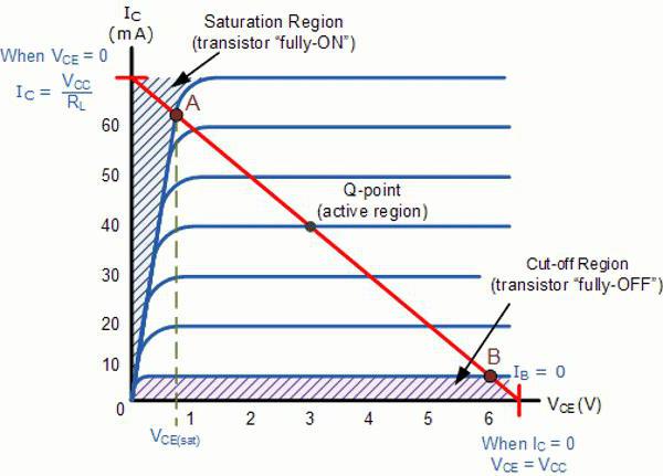
They can be clearly demonstrated if a circuit for switching on a bipolar transistor with an OE is assembled.
If you plot on the ordinate and abscissa axes the segments corresponding to the maximum possible collector current and the value of the supply voltage V CC, and then connect their ends to each other, you will get a load line (red). It is described by the expression: I C = (V CC - V CE)/R C. It follows from the figure that the operating point, which determines the collector current IC and voltage V CE, will shift along the load line from bottom to top as the base current I V increases.
The area between the V CE axis and the first output characteristic (shaded), where I B = 0, characterizes the cutoff mode. In this case, the reverse current I C is negligible, and the transistor is closed.
The uppermost characteristic at point A intersects with the direct load, after which, with a further increase in I B, the collector current no longer changes. The saturation zone on the graph is the shaded area between the I C axis and the steepest characteristic.
How does a transistor behave in different modes?
The transistor operates with variable or constant signals entering the input circuit.
Bipolar transistor: switching circuits, amplifier
For the most part, the transistor serves as an amplifier. An alternating signal at the input causes its output current to change. Here you can use schemes with OK or with OE. The signal requires a load in the output circuit. Typically a resistor is used in the output collector circuit. If it is chosen correctly, the output voltage will be significantly higher than the input.
The operation of the amplifier is clearly visible in the timing diagrams.

When pulse signals are converted, the mode remains the same as for sinusoidal ones. The quality of conversion of their harmonic components is determined by the frequency characteristics of the transistors.
Operation in switching mode
Designed for contactless switching of connections in electrical circuits. The principle is to change the resistance of the transistor in steps. The bipolar type is quite suitable for the requirements of the key device.
Conclusion
Semiconductor elements are used in electrical signal conversion circuits. Universal capabilities and large classification allow bipolar transistors to be widely used. Switching circuits determine their functions and operating modes. Much also depends on the characteristics.
The basic switching circuits of bipolar transistors amplify, generate and convert input signals, and also switch electrical circuits.
Whenever a transistor is connected to a circuit, input and output current will flow through one of its terminals; this terminal is called common.
There are three schemes for switching on a bipolar transistor:
- with a common emitter;
- with a common collector;
- with a common base;
- high current gain;


In all waveforms in the article, the first channel is the input signal, the second channel is the output signal. The input signal is taken after the coupling capacitor, otherwise the capacitor introduces a phase shift.
The oscillogram shows that the amplitude of the output signal is several times greater than the amplitude of the input signal, while the output signal is inverted relative to the input signal, this means that when the input signal increases, the output decreases and vice versa. The diagram shows a capacitor with a dotted line; it can be connected if you need to increase the gain. Let's connect it.

We see that the output signal has increased by approximately an order of magnitude, that is, 10 times. This transistor connection circuit is used in power amplifiers.
When the capacitor was turned on, the input resistance of the circuit decreased, which led to distortion of the generator signal, and consequently the output signal.
Circuit with a common collector.
- the input signal is sent to the base;
- the output signal is removed from the emitter;
- high current gain;
- input and output signal voltages differ by approximately 0.6 V;

Let's assemble the circuit drawn above and see how the output signal will change depending on the input.

The oscillogram shows that the amplitudes of the signals are equal because the oscilloscope displays only the AC component; if you turn on the oscilloscope to display the DC component, the difference between the signal at the input and output will be 0.6 V. The circuit does not invert the signal and is used as a buffer or for coordination of cascades.
In electronics, a buffer is a circuit that increases the load capacity of a signal, that is, the signal remains the same shape, but is capable of delivering more current.
Scheme with a common base.
- the input signal is sent to the emitter;
- the output signal is removed from the collector;
- high voltage gain;
- current gain is close to zero, the emitter current is greater than the collector current by the base current;

Let's assemble the circuit drawn above and see how the output signal will change depending on the input.

The oscillogram shows that the amplitude of the output signal is approximately ten times greater than the amplitude of the input signal, and the output signal is not inverted relative to the input signal. This transistor connection circuit is used in radio frequency amplifiers. A common-base cascade has a low input impedance, so the generator signal is distorted, and therefore the output signal too.
The question arises: why not use a common emitter circuit to amplify radio frequencies, since it increases the amplitude of the signal? It's all about the capacitance of the base-collector junction, it is also called the Miller capacitance. For radio frequencies, this capacitance has low resistance, so the signal, instead of flowing through the base-emitter junction, passes through this capacitance and flows to ground through the open transistor. How this happens is shown in the figure below.

Perhaps this is all I wanted to tell you about the transistor switching circuits.
Transistors are divided into bipolar and field-effect. Each of these types has its own operating principle and design, however, what they have in common is the presence of semiconductor p-n structures.
Symbols of transistors are given in the table:
| Device type | Conventional graphic symbol (UGO) |
|||
|---|---|---|---|---|
| Bipolar | Bipolar pnp type | |||
| Bipolar n-p-n type | ||||
| Field | With the manager p-n junction | With p-type channel | ||
| With n-type channel | ||||
| With isolated shutter MOSFET transistors | With built-in channel | Built-in channel p-type | ||
| Built-in channel n-type | ||||
| With induced channel | Induced channel p-type | |||
| Induced channel n-type | ||||
Bipolar transistors
The definition of “bipolar” indicates that the operation of a transistor is associated with processes in which charge carriers of two types take part - electrons and holes.
A transistor is a semiconductor device with two electron-hole junctions, designed to amplify and generate electrical signals. A transistor uses both types of carriers - major and minor, which is why it is called bipolar.
A bipolar transistor consists of three regions of a monocrystalline semiconductor with different types of conductivity: emitter, base and collector.

- E - emitter,
- B - base,
- K - collector,
- EP - emitter junction,
- KP - collector junction,
- W - base thickness.
Each of the transitions of the transistor can be turned on either in the forward or reverse direction. Depending on this, there are three operating modes of the transistor:
- Cut-off mode - both p-n junctions are closed, while a relatively small current usually flows through the transistor
- Saturation mode - both p-n junctions are open
- Active mode - one of the p-n junctions is open and the other is closed
In cutoff mode and saturation mode, the transistor cannot be controlled. Effective control of the transistor is carried out only in active mode. This mode is the main one. If the voltage at the emitter junction is direct, and at the collector junction it is reverse, then the switching on of the transistor is considered normal; if the polarity is opposite, it is inverse.
In normal mode, the collector p-n junction is closed, the emitter junction is open. The collector current is proportional to the base current.
The movement of charge carriers in an n-p-n transistor is shown in the figure:

When the emitter is connected to the negative terminal of the power source, an emitter current Ie occurs. Since an external voltage is applied to the emitter junction in the forward direction, the electrons cross the junction and enter the base region. The base is made of a p-semiconductor, so electrons are minority charge carriers for it.
Electrons that enter the base region partially recombine with holes in the base. However, the base is usually made of a very thin p-conductor with a high resistivity (low impurity content), so the concentration of holes in the base is low and only a few electrons entering the base recombine with its holes, forming a base current Ib. Most electrons, due to thermal motion (diffusion) and under the influence of the collector field (drift), reach the collector, forming a component of the collector current Ik.
The relationship between the increments of the emitter and collector currents is characterized by the current transfer coefficient

As follows from a qualitative examination of the processes occurring in a bipolar transistor, the current transfer coefficient is always less than unity. For modern bipolar transistors α = 0.9 ÷ 0.95
When Ie ≠ 0, the transistor collector current is equal to:
![]()
In the considered connection circuit, the base electrode is common to the emitter and collector circuits. This circuit for connecting a bipolar transistor is called a circuit with a common base, while the emitter circuit is called the input circuit, and the collector circuit is called the output circuit. However, such a circuit for switching on a bipolar transistor is used very rarely.
Three circuits for switching on a bipolar transistor
There are switching circuits with a common base, a common emitter, and a common collector. Circuits for a pnp transistor are shown in figures a, b, c:

In a circuit with a common base (Fig. a), the base electrode is common to the input and output circuits; in a circuit with a common emitter (Fig. b), the emitter is common; in a circuit with a common collector (Fig. c), the collector is common.
The figure shows: E1 – power supply of the input circuit, E2 – power supply of the output circuit, Uin – source of the amplified signal.
The main switching circuit is one in which the common electrode for the input and output circuits is the emitter (switching circuit for a bipolar transistor with a common emitter). For such a circuit, the input circuit passes through the base-emitter junction and a base current arises in it:
The low value of the base current in the input circuit has led to the widespread use of a common emitter circuit.
Bipolar transistor in a common emitter (CE) circuit
In a transistor connected according to the OE circuit, the relationship between current and voltage in the input circuit of the transistor Ib = f1 (Ube) is called the input or basic current-voltage characteristic (VC) of the transistor. The dependence of the collector current on the voltage between the collector and the emitter at fixed values of the base current Iк = f2 (Uke), Ib – const is called the family of output (collector) characteristics of the transistor.
The input and output current-voltage characteristics of a medium-power bipolar transistor of the n-p-n type are shown in the figure:

As can be seen from the figure, the input characteristic is practically independent of the voltage Uke. The output characteristics are approximately equidistant from each other and almost linear over a wide range of voltage changes Uke.
The dependence Ib = f(Ube) is an exponential dependence characteristic of the current of a forward-biased p-n junction. Since the base current is recombination, its value Ib is β times less than the injected emitter current Ie. As the collector voltage Uк increases, the input characteristic shifts to the region of higher voltages Ub. This is due to the fact that due to modulation of the base width (Early effect), the proportion of recombination current in the base of the bipolar transistor decreases. The voltage Ube does not exceed 0.6...0.8 V. Exceeding this value will lead to a sharp increase in the current flowing through the open emitter junction.
The dependence Ik = f(Uke) shows that the collector current is directly proportional to the base current: Ik = B Ib
Bipolar transistor parameters
Representation of a transistor in a small-signal mode of operation as a four-terminal network
In a small-signal operating mode, the transistor can be represented by a four-terminal network. When voltages u1, u2 and currents i1, i2 change according to a sinusoidal law, the connection between voltages and currents is established using Z, Y, h parameters.

Potentials 1", 2", 3 are the same. It is convenient to describe a transistor using h-parameters.
The electrical state of a transistor connected according to a circuit with a common emitter is characterized by four quantities: Ib, Ube, Ik and Uke. Two of these quantities can be considered independent, and the other two can be expressed in terms of them. For practical reasons, it is convenient to choose the quantities Ib and Uke as independent ones. Then Ube = f1 (Ib, Uke) and Ik = f2 (Ib, Uke).
In amplifying devices, the input signals are increments of input voltages and currents. Within the linear part of the characteristics, the following equalities are true for the increments Ube and Ik:

Physical meaning of the parameters:

For a circuit with OE, the coefficients are written with the index E: h11e, h12e, h21e, h22e.
The passport data indicates h21е = β, h21b = α. These parameters characterize the quality of the transistor. To increase the value of h21, you need to either reduce the base width W or increase the diffusion length, which is quite difficult.
Composite transistors
To increase the value of h21, bipolar transistors are connected using a Darlington circuit:

In a composite transistor that has the same characteristics as one, the base VT1 is connected to the emitter VT2 and ΔIе2 = ΔIb1. The collectors of both transistors are connected and this terminal is the terminal of the composite transistor. The base VT2 plays the role of the base of the composite transistor ΔIb = ΔIb2, and the emitter VT1 plays the role of the emitter of the composite transistor ΔIe = ΔI1.
Let us obtain an expression for the current gain β for the Darlington circuit. Let us express the relationship between the change in the base current dIb and the resulting change in the collector current dIk of the composite transistor as follows:

Since for bipolar transistors the current gain is usually several tens (β1, β2 >> 1), the total gain of the composite transistor will be determined by the product of the gains of each transistor βΣ = β1 · β2 and can be quite large in value.
Let us note the features of the operating mode of such transistors. Since the emitter current VT2 Ie2 is the base current VT1 dIb1, then, therefore, transistor VT2 should operate in micro-power mode, and transistor VT1 - in high-injection mode, their emitter currents differ by 1-2 orders of magnitude. With such a suboptimal choice of operating characteristics of bipolar transistors VT1 and VT2, it is not possible to achieve high current gain values in each of them. Nevertheless, even with gain values β1, β2 ≈ 30, the total gain βΣ will be βΣ ≈ 1000.
High gain values in composite transistors are realized only in statistical mode, so composite transistors are widely used in the input stages of operational amplifiers. In circuits at high frequencies, composite transistors no longer have such advantages; on the contrary, both the limiting current amplification frequency and the operating speed of the composite transistors are less than the same parameters for each of the transistors VT1, VT2 separately.
Frequency properties of bipolar transistors
The process of propagation of minority charge carriers injected into the base from the emitter to the collector junction proceeds by diffusion. This process is quite slow, and the carriers injected from the emitter will reach the collector no earlier than during the diffusion of carriers through the base. Such a delay will lead to a phase shift between the current Ie and the current Ik. At low frequencies, the phases of the currents Ie, Ik and Ib coincide.
The frequency of the input signal at which the modulus of the gain decreases by a factor of compared to the static value β0 is called the limiting frequency of current amplification of a bipolar transistor in a common-emitter circuit


Fβ – limiting frequency (cutoff frequency)
fgr – cut-off frequency (unity gain frequency)
Field effect transistors
Field-effect, or unipolar, transistors use the field effect as the main physical principle. Unlike bipolar transistors, in which both types of carriers, both major and minor, are responsible for the transistor effect, field-effect transistors use only one type of carrier to realize the transistor effect. For this reason, field-effect transistors are called unipolar. Depending on the conditions for implementing the field effect, field-effect transistors are divided into two classes: field-effect transistors with an insulated gate and field-effect transistors with a control p-n junction.
Field-effect transistors with control p-n junction
Schematically, a field-effect transistor with a control pn junction can be represented as a plate, to the ends of which electrodes, a source and a drain are connected. In Fig. shows the structure and connection diagram of a field-effect transistor with an n-type channel:

In an n-channel transistor, the majority charge carriers in the channel are electrons, which move along the channel from a low-potential source to a higher-potential drain, producing a drain current Ic. A voltage is applied between the gate and the source, blocking the p-n junction formed by the n-region of the channel and the p-region of the gate.
When a blocking voltage is applied to the p-n junction Uzi, a uniform layer appears at the channel boundaries, depleted of charge carriers and having a high resistivity. This leads to a decrease in the conductive width of the channel.
By changing the value of this voltage, it is possible to change the cross-section of the channel and, consequently, change the value of the electrical resistance of the channel. For an n-channel field effect transistor, the drain potential is positive with respect to the source potential. When the gate is grounded, current flows from drain to source. Therefore, to stop the current, a reverse voltage of several volts must be applied to the gate.
The voltage value Uzi, at which the current through the channel becomes almost equal to zero, is called the cut-off voltage Uzap
Thus, a field-effect transistor with a gate in the form of a p-n junction represents a resistance, the value of which is regulated by an external voltage.
The field-effect transistor is characterized by the following current-voltage characteristic:

Here, the dependence of the drain current Ic on the voltage at a constant voltage at the gate Uzi determines the output, or drain, characteristics of the field-effect transistor. At the initial section of the characteristics Usi + |Uzi |< Uзап ток стока Iс возрастает с увеличением Uси . При повышении напряжения сток - исток до Uси = Uзап - |Uзи | происходит перекрытие канала и дальнейший рост тока Iс прекращается (участок насыщения). Отрицательное напряжение Uзи между затвором и истоком смещает момент перекрытия канала в сторону меньших значений напряжения Uси и тока стока Iс . Участок насыщения является рабочей областью выходных характеристик полевого транзистора. Дальнейшее увеличение напряжения Uси приводит к пробою р-n-перехода между затвором и каналом и выводит транзистор из строя.
The current-voltage characteristic Ic = f(Uzi) shows the voltage Uzap. Since Uzi ≤ 0 the p-n junction is closed and the gate current is very small, about 10 -8…10-9 A, therefore, the main advantages of a field-effect transistor, compared to a bipolar transistor, include a high input resistance, about 10 10…1013 Ohm. In addition, they are distinguished by low noise and manufacturability.
There are two main switching schemes that have practical application. A circuit with a common source (Fig. a) and a circuit with a common drain (Fig. b), which are shown in the figure:

Insulated gate field effect transistors
(MOS transistors)
The term "MOS transistor" is used to refer to field-effect transistors in which the control electrode - the gate - is separated from the active region of the field-effect transistor by a dielectric layer - an insulator. The basic element for these transistors is the metal-insulator-semiconductor (M-D-S) structure.
The technology of an MOS transistor with a built-in gate is shown in the figure:

The original semiconductor on which the MOS transistor is made is called the substrate (pin P). The two heavily doped n+ regions are called source (I) and drain (C). The area of the substrate under the gate (3) is called the embedded channel (n-channel).
The physical basis for the operation of a field-effect transistor with a metal-insulator-semiconductor structure is the field effect. The field effect is that under the influence of an external electric field the concentration of free charge carriers in the near-surface region of the semiconductor changes. In field devices with an MIS structure, the external field is caused by the applied voltage to the metal gate electrode. Depending on the sign and magnitude of the applied voltage, there can be two states of the space charge region (SCR) in the channel - enrichment, depletion.
The depletion mode corresponds to a negative voltage Uzi, at which the electron concentration in the channel decreases, which leads to a decrease in the drain current. The enrichment mode corresponds to a positive voltage Uzi and an increase in drain current.
The current-voltage characteristic is shown in the figure:

The topology of an MOS transistor with an induced (induced) p-type channel is shown in the figure:

When Uzi = 0 there is no channel and Ic = 0. The transistor can only operate in Uzi enrichment mode< 0. Если отрицательное напряжение Uзи превысит пороговое Uзи.пор , то происходит формирование инверсионного канала. Изменяя величину напряжения на затворе Uзи в области выше порогового Uзи.пор , можно менять концентрацию свободных носителей в инверсионном канале и сопротивление канала. Источник напряжения в стоковой цепи Uси вызовет ток стока Iс .
The current-voltage characteristic is shown in the figure:

In MOS transistors, the gate is separated from the semiconductor by a layer of SiO2 oxide. Therefore, the input resistance of such transistors is about 1013 ... 1015 Ohms.
The main parameters of field-effect transistors include:
- The slope of the characteristic at Usp = const, Upi = const. Typical parameter values are (0.1...500) mA/V;
- The slope of the characteristic along the substrate at Usp = const, Uzi = const. Typical parameter values (0.1...1) mA/V;
- Initial drain current Is.init.
- – drain current at zero voltage value Uzi. Typical parameter values: (0.2...600) mA – for transistors with a control channel p-n junction; (0.1...100) mA – for transistors with a built-in channel; (0.01...0.5) µA – for transistors with an induced channel;
- Cut-off voltage Uzi.ots. . Typical values (0.2...10) V; threshold voltage Up. Typical values (1...6) V;
- Drain-source resistance in open state. Typical values (2..300) Ohm
- Differential resistance (internal): at Uzi = const;
- Ia – anode current (power current in the anode-cathode circuit of the thyristor);
- Uak – voltage between anode and cathode;
- Iу – control electrode current (in real circuits current pulses are used);
- Uuk is the voltage between the control electrode and the cathode;
- Upit – supply voltage.
Statistical gain: μ = S ri
Thyristors
A thyristor is a semiconductor device with three or more electron-hole p-n junctions. They are mainly used as electronic keys. Depending on the number of external terminals, they are divided into thyristors with two external terminals - dinistors and thyristors with three terminals - thyristors. The letter symbol VS is used to designate thyristors.
The structure, UGO and current-voltage characteristics of the dinistor are shown in the figure:

The outer p-region is called the anode (A), the outer n-region is called the cathode (K). Three p-n junctions are designated by numbers 1, 2, 3. The structure of the dinistor is 4-layer - p-n-p-n.
The supply voltage E is supplied to the dinistor in such a way that 1 of the 3 junctions is open and their resistance is insignificant, and transition 2 is closed and all the supply voltage Upr is applied to it. A small reverse current flows through the dinistor, the load R is disconnected from the power source E.
When a critical voltage is reached equal to the switch-on voltage Uon, transition 2 opens, while all three transitions 1, 2, 3 will be in the open (on) state. The resistance of the dinistor drops to tenths of an ohm.
The turn-on voltage is several hundred volts. The dinistor opens and significant currents flow through it. The voltage drop across the dinistor in the open state is 1-2 volts and depends little on the magnitude of the flowing current, the value of which is τa ≈ E / R, and UR ≈ E, i.e. the load is connected to the power source E. The voltage across the dinistor, corresponding to the maximum permissible point Iopen.max, is called the open state voltage Uokr. The maximum permissible current ranges from hundreds of mA to hundreds of A. The dinistor is in the open state until the current flowing through it becomes less than the holding current Iud. The dinistor closes when the external voltage decreases to a value of the order of 1V or when the polarity of the external source changes. Therefore, such a device is used in transient current circuits. Points B and D correspond to the limit values of dinistor currents and voltages. The recovery time of transition 2 resistance after removing the supply voltage is about 10-30 μs.
By their principle, dinistors are key action devices. In the on state (BV section) it is similar to a closed key, and in the off state (EG section) it is like an open key.
The design and principle of operation of a thyristor (thyristor)
The thyristor is a controlled device. It contains a control electrode (CE) connected to a p-type semiconductor or an n-type semiconductor of the middle junction 2.
The structure, UGO and current-voltage characteristics of a trinistor (usually called a thyristor) are shown in the figure:

The voltage Uoff, at which an avalanche-like increase in current begins, can be reduced by introducing minority charge carriers into any of the layers adjacent to junction 2. The extent to which Uon decreases is shown on the current-voltage characteristic. An important parameter is the unlocking control current Iу.оt, which ensures that the thyristor switches to the open state at voltages lower than the voltage Uon. The figure shows three values of switching voltage UI on< Un вкл < Um вкл соответствует трем значениям управляющего тока UI у.от >Un u.ot > Um u.ot .
Let's consider the simplest circuit with a thyristor loaded onto a resistor load Rн
To transfer the thyristor to the open state, the non-control electrode is supplied from the pulse generation circuit with a short-term (on the order of several microseconds) control pulse.
A characteristic feature of the non-lockable thyristor in question, which is very widely used in practice, is that it cannot be turned off using the control current.
To turn off the thyristor in practice, reverse voltage Uac is applied to it< 0 и поддерживают это напряжение в течении времени, большего так называемого времени выключения tвыкл . Оно обычно составляет единицы или десятки микросекунд.
The design and principle of operation of a triac
So-called symmetrical thyristors (triacs, triacs) are widely used. Each triac is similar to a pair of the considered thyristors, connected back-to-back. Symmetrical thyristors are a controlled device with a symmetrical current-voltage characteristic. To obtain a symmetrical characteristic, double-sided p-n-p-n-p semiconductor structures are used.
The structure of the triac, its UGO and current-voltage characteristics are shown in the figure:

A triac (triac) contains two thyristors p1-n1-p2-n2 and p2-n2-p1-n4 connected back-to-back. The triac contains 5 transitions P1-P2-P3-P4-P5. In the absence of a control electron, the UE triac is called a diac.
With positive polarity on electrode E1, a thyristor effect occurs in p1-n1-p2-n2, and with opposite polarity in p2-n1-p1-n4.
When a control voltage is applied to the UE, depending on its polarity and magnitude, the switch voltage Uon changes
Thyristors (dinistors, thyristors, triacs) are the main elements in power electronics devices. There are thyristors for which the switching voltage is greater than 1 kV, and the maximum permissible current is greater than 1 kA
Electronic keys
To increase the efficiency of power electronics devices, the pulsed operating mode of diodes, transistors and thyristors is widely used. The pulse mode is characterized by sudden changes in currents and voltages. In pulse mode, diodes, transistors and thyristors are used as switches.
Using electronic keys, electronic circuits are switched: connecting/disconnecting a circuit to/from sources(s) of electrical energy or signal, connecting or disconnecting circuit elements, changing the parameters of circuit elements, changing the type of the influencing signal source.
UGO ideal keys are shown in the figure:
Keys that operate to open and close, respectively.
The key mode is characterized by two states: “on”/“off”.
Ideal keys are characterized by an instantaneous change in resistance, which can take the value 0 or ∞. The voltage drop across an ideal closed switch is 0. When the switch is open, the current is 0.
Real keys are also characterized by two extreme resistance values Rmax and Rmin. The transition from one resistance value to another in real switches occurs in a finite time. The voltage drop across a real closed switch is not zero.
The switches are divided into keys used in low-power circuits and keys used in high-power circuits. Each of these classes has its own characteristics.
The keys used in low-power circuits are characterized by:
- Key resistances in open and closed states;
- Performance – the time it takes for a key to transition from one state to another;
- Voltage drop on a closed switch and leakage current on an open switch;
- Noise immunity – the ability of a key to remain in one of the states when exposed to interference;
- The sensitivity of the key is the magnitude of the control signal that transfers the key from one state to another;
- Threshold voltage – the value of the control voltage, in the vicinity of which there is a sharp change in the resistance of the electronic key.
Diode electronic keys
The simplest type of electronic keys is diode switches. The diode switch circuit, static transfer characteristic, current-voltage characteristic and the dependence of the differential resistance on the diode voltage are shown in the figure:


The principle of operation of a diode electronic switch is based on changing the value of the differential resistance of a semiconductor diode in the vicinity of the threshold voltage value on the diode Uthr. Figure "c" shows the current-voltage characteristic of a semiconductor diode, which shows the value of Uthr. This value is located at the intersection of the voltage axis with the tangent drawn to the ascending member of the current-voltage characteristic.
Figure "d" shows the dependence of the differential resistance on the voltage across the diode. It follows from the figure that in the vicinity of the threshold voltage of 0.3 V there is a sharp change in the differential resistance of the diode with extreme values of 900 and 35 Ohms (Rmin = 35 Ohms, Rmax = 900 Ohms).
In the “on” state, the diode is open and Uout ≈ Uin.
In the “off” state, the diode is closed and , Uout ≈ Uin · Rн / Rmax< In order to reduce the switching time, diodes with a low transition capacitance of the order of 0.5-2 pF are used, while providing a turn-off time of the order of 0.5-0.05 μs. Diode switches do not allow electrical separation of the control and controlled circuits, which is often required in practical circuits. The majority of circuits used in computers, remote control devices, automatic control systems, etc. are based on transistor switches. The switch circuits on the bipolar transistor and the current-voltage characteristics are shown in the figure: The first state “off” (transistor closed) is determined by point A1 on the output characteristics of the transistor; it is called cutoff mode. In the cutoff mode, the base current Ib = 0, the collector current Ik1 is equal to the initial collector current, and the collector voltage Uk = Uk1 ≈ Ek. The cutoff mode is implemented at Uin = 0 or at negative base potentials. In this state, the switch resistance reaches its maximum value: Rmax = , where RT is the transistor resistance in the closed state, more than 1 MOhm. The second state “on” (the transistor is open) is determined by point A2 on the current-voltage characteristic and is called the saturation mode. From the cutoff mode (A1) to the saturation mode (A2), the transistor is switched by a positive input voltage Uin. In this case, the voltage Uout takes a minimum value Uk2 = Uk.e.us of the order of 0.2-1.0 V, the collector current Ik2 = Ik.us ≈ Ek / Rk. The base current in saturation mode is determined from the condition: Ib > Ib.us = Ik.us / h21. The input voltage required to switch the transistor to the open state is determined from the condition: U in > Ib.us · Rb + Uk.e.us Good noise immunity and low power dissipation in the transistor are explained by the fact that most of the time the transistor is either saturated (A2) or closed (A1), and the transition time from one state to another is a small part of the duration of these states. The switching time of switches on bipolar transistors is determined by the barrier capacitances of the p-n junctions and the processes of accumulation and resorption of minority charge carriers in the base. To increase speed and input resistance, field-effect transistor switches are used. Switch circuits on field-effect transistors with a control pn junction and with an induced channel with a common source and common drain are shown in the figure: For any switch on a field-effect transistor Rн > 10-100 kOhm. The control signal Uin at the gate is about 10-15 V. The resistance of the field-effect transistor in the closed state is high, about 108 -109 Ohms. The resistance of the field-effect transistor in the open state can be 7-30 Ohms. The resistance of the field-effect transistor along the control circuit can be 108 -109 Ohms. (schemes “a” and “b”) and 1012 -1014 Ohms (schemes “c” and “d”). Power semiconductor devices are used in energy electronics, the most rapidly developing and promising field of technology. They are designed to control currents of tens and hundreds of amperes, voltages of tens and hundreds of volts. Power semiconductor devices include thyristors (dinistors, thyristors, triacs), transistors (bipolar and field-effect) and statically induced bipolar transistors (IGBT). They are used as electronic keys that switch electronic circuits. They try to bring their characteristics closer to the characteristics of ideal keys. According to the principle of operation, characteristics and parameters, high-power transistors are similar to low-power transistors, but there are certain features. Currently, the field-effect transistor is one of the most promising power devices. The most widely used transistors are insulated gate and induced channel transistors. To reduce the channel resistance, its length is reduced. To increase the drain current, hundreds and thousands of channels are made in the transistor, and the channels are connected in parallel. The probability of self-heating of the field-effect transistor is small, because The channel resistance increases with increasing temperature. Power field-effect transistors have a vertical structure. Channels can be located both vertically and horizontally. This MOS transistor, manufactured by the double diffusion method, has a horizontal channel. The figure shows a structure element containing a channel. This V-shaped MOS transistor has a vertical channel. The figure shows one structure element containing two channels. It is easy to see that the structures of a VMOS transistor and a DMIS transistor are similar. IGBT is a hybrid semiconductor device. It combines two methods of controlling electric current, one of which is typical for field-effect transistors (control of the electric field), and the second for bipolar ones (control of the injection of electrical carriers). Typically, IGBTs use an n-type induced channel MOS transistor structure. The structure of this transistor differs from the structure of a DMIS transistor by an additional layer of p-type semiconductor. Please note that the terms “emitter”, “collector” and “gate” are commonly used to refer to IGBT electrodes. Adding a p-type layer results in the formation of a second bipolar transistor structure (pnp type). Thus, IGBT has two bipolar structures - n-p-n type and p-n-p type. The UGO and the IGBT switch-off circuit are shown in the figure: A typical type of output characteristics is shown in the figure: SIT is a field-effect transistor with a control p-n junction with static induction. It is multi-channel and has a vertical structure. The schematic representation of the SIT and the common source circuit are shown in the figure: The regions of a p-type semiconductor have the shape of cylinders, the diameter of which is a few micrometers or more. This cylinder system acts as a shutter. Each cylinder is connected to a gate electrode (in figure “a” the gate electrode is not shown). The dotted lines indicate the areas of p-n junctions. The actual number of channels can be thousands. Typically SIT is used in common source circuits. Each of the devices considered has its own area of application. Thyristor switches are used in devices operating at low frequencies (kilohertz and below). The main disadvantage of such keys is their low performance. The main area of application of thyristors are low-frequency devices with high switching power up to several megawatts, which do not impose serious performance requirements. Powerful bipolar transistors are used as high-voltage switches in devices with a switching or conversion frequency in the range of 10-100 kHz, with an output power level from a few W to several kW. The optimal range of switching voltages is 200-2000 V. Field-effect transistors (MOSFETs) are used as electronic switches for switching low-voltage, high-frequency devices. The optimal values of switching voltages do not exceed 200 V (maximum value up to 1000 V), while the switching frequency can range from a few kHz to 105 kHz. The range of switched currents is 1.5-100 A. The positive properties of this device are controllability by voltage, not current, and less dependence on temperature compared to other devices. Insulated gate bipolar transistors (IGBTs) are used at frequencies below 20 kHz (some types of devices are used at frequencies above 100 kHz) with switching powers above 1 kW. Switched voltages are not lower than 300-400 V. Optimal values of switched voltages are above 2000 V. IGBT and MOSFET require a voltage of no higher than 12-15 V for full switching on; negative voltage is not required to close the devices. They are characterized by high switching speeds. Amplifiers contain transistors, as well as elements such as resistors, capacitors and inductors. The parameters of the elements used (their ratings and voltages) depend on the requirements for the amplifier, as well as on the type of transistors used. With the advent of various types of transistors, new amplifier circuit configurations became possible. In biopolar R -n- R- or n - R -n-transistor creates alternating regions with different types of conductivity in a certain order, forming a base, emitter and collector. The transistor is called bipolar, since charge transfer in it is carried out by both electrons and holes. IN field or (unipolar) In transistors, charges are carried by carriers of one type: either electrons or holes. Field-effect transistors (FETs) have three regions called gate, source and drain. Depending on the type of media used, there are two types of field-effect transistors: R- and I-channel. Different types of transistors have different characteristics, which are described in more detail in this section. The most common circuit for constructing an amplifier based on a bipolar transistor is a circuit with a common (grounded) emitter (CE); Variants of such schemes are shown in Fig. 11.1. The term "common emitter" indicates that in a suitable circuit the resistance between the emitter terminal and ground is low for a signal, but it does not follow that it is low in all cases for DC. So, for example, in the diagrams shown in Fig. 1.1, A And b, the emitters are directly grounded, and in the circuit in Fig. 1.1, a resistance is connected between the emitter and the ground, shunted by a capacitor. Therefore, if the reactance of this capacitor for the signal is small, we can assume that the emitter is practically grounded for the signal. To operate in class A (section 1.4), the bias voltage between the base and emitter must be forward (unlocking), and between the collector and emitter - reverse (blocking). To achieve this bias, the polarity of the power supplies is selected depending on the type of transistor used. For transistor R -n -
p-type (Fig. 11 L, a) the plus of the bias source must be connected to the p-type emitter, and the minus to the i-type base. Thus, forward bias is obtained at a negative base potential relative to the emitter. To reverse bias a p-type collector, its potential must be negative. To do this, the power source is connected with the positive pole to the emitter, and the negative pole to the collector. The input signal creates across a resistor R 1
voltage drop, which is algebraically added to the constant bias voltage. As a result, the total base potential changes in accordance with the signal. As the base potential changes, the collector current changes, and therefore the voltage across the resistor R2.
With a positive half-wave of the input voltage, the forward bias decreases and the current through R 2
decreases accordingly. Voltage drop per R 2
also decreases, resulting in a 180° phase shift between the input and output signals. If transistor n is used - R- n-type (Fig. 1.1.6), then the polarity of both power sources is reversed. In this case, the base junction also turns out to be biased in the forward direction, and the collector junction in the opposite direction. As in the previous case, a phase shift of 180° is formed between the input and output signals. In Fig. 1.1, a and b show the main elements of the amplifier, and the amplifier circuit used in practice is shown in Fig. 1.1.6. Here, capacitor C 1 does not allow the constant component of the input signal to pass through, but has a low reactance for its variable component, which is thus supplied to the resistor R 2
.
(This is the so-called R.C.-connection; it is described in more detail in section. 1.5). Base forward bias voltage comes from voltage divider Ri- R2, which is connected to the power source. The required forward bias value of the transistor base is obtained by properly choosing the ratio of the resistance values R 1
And R 2
.
Moreover, in the transistor n - R- n-type base potential is set more positive than the emitter. The collector resistor on which the output signal is generated is usually called a load resistor and is designated R n. Through the isolation capacitor C 3, the signal is sent to the next stage. Input and output circuits must have a common grounded point (Fig. 1.1, A). The base current amplification factor for a circuit with OE is given by the following relation: where p is the base current amplification factor; DI b - base current increment; DI k - the corresponding increment in the collector current at - Rice. 1.1. Common emitter circuits. Thus, p is equal to the ratio of the increment of the collector current to the corresponding increment of the base current at a constant collector voltage. The signal current gain is also called direct current transfer coefficient [ With a sufficiently large resistance value R 2
the alternating component of the signal current is practically equal to the alternating component of the base current. - Note ed.]
Resistor R 3 (Fig. 1.1.5) has a stabilizing effect on the transistor current when the temperature changes. The voltage drop across R 3 creates a reverse (turn-off) bias at the emitter junction of the transistor, as it increases the emitter potential. Therefore, it reduces the positive forward base bias by the amount of this voltage drop. The presence of an alternating voltage component on Rz would cause a decrease in the output signal and, consequently, the gain of the amplifier (see Section 1.8). To eliminate this effect, resistor Rз is shunted with capacitor C2. When the transistor heats up, the DC component of the collector current increases. Accordingly, the voltage drop across Rz,
which results in a reduction in forward base bias as well as collector current. As a result, partial compensation of the temperature drift of the current is carried out. In Fig. Figure 1.2 shows a field-effect transistor amplifier circuit equivalent to an OE circuit, which is called a common-source circuit. In this circuit, the gate corresponds to the base of the bipolar transistor, the source to the emitter, and the drain to the collector. In diagram 1.2, A FET with n-type channel is shown. For a transistor with a p-type channel, the arrow on the gate will be directed in the opposite direction. In Fig. 1.2, b also shows a transistor with a d-type channel, and in Fig. 1.2, V- with a p-type channel. FET bias circuits differ from bipolar transistor bias circuits due to significant differences in the characteristics of these devices. Bipolar transistors are amplifiers signal current and reproduce at the output the amplified input signal current, while in field-effect transistors the output signal current is controlled by the one applied to the input signal voltage. There are two types of PT: with control R- n-junction and metal-oxide-semiconductor (MOS). (MOS transistors are also called insulated gate field effect transistors.) Both types of field effect transistors are made with n –
and p-channels. In the diagram in Fig. 1.2, and a PT with a control is used R- I-transition, and in the diagram in Fig. 1.2, b - MOS transistor operating in enrichment mode. In Fig. 1.2, V shows a MOSFET operating in depletion mode. In MOS transistors, the gate is depicted as a capacitor plate, which symbolizes the capacitance resulting from the formation of a very thin oxide layer that insulates the metal contact of the gate terminal from the channel. (The term "MOS transistor" comes from this production method.) Since FETs are driven by input voltage rather than current like bipolar transistors, the signal current gain parameter is replaced by conductance g m.
Transfer conductance is a measure of the quality of a field effect transistor and characterizes the ability of the gate voltage to drive drain current. The expression for transfer conductivity is as follows: Unit g m,
called siemens, is the reciprocal of the unit of resistance (1 cm = 1/ohm). As follows from expression (1.2), the parameter g m
for a FET, it is the ratio of the drain current increment to the gate voltage increment at a constant voltage between source and drain. In a field-effect transistor with a control R- n-junction and n-type channel (Fig. 1.2, a) when a negative voltage is applied to the gate, the channel is depleted of charge carriers and the channel conductivity decreases. (For a p-channel FET, the conductivity decreases when a positive voltage is applied to the gate.) Since a unijunction FET has only two zones with different conduction types (the source and drain terminals are connected to one zone, and the gate terminal to the other), the conductivity between source and drain of the same type as the conductivity of the channel. Therefore, unlike a bipolar transistor, which has U Q 3
=
0 collector current is 0, channel current can flow even at zero gate-source voltage. Since the channel current is a function of the voltage Uzi, the field-effect transistor channel with the control R- an n-junction can conduct current in both directions: from source to drain and in the opposite direction (in a bipolar transistor, the collector current in operating mode always has one direction). In this case, the operating point (for example, for class A circuits) for such transistors is set by applying voltage reverse bias gate, in contrast to forward biasing of the base junction in bipolar transistors [In a transistor with a control R- an n-junction usually applies a blocking voltage U 8i to the junction (negative for the n-channel) and the maximum current in the channel is obtained at U 3 i = 0. The direction of the current in the channel depends on the polarity of the power source connected to the channel; When the polarity of the power supply is reversed, the terminal that was the drain becomes the source and vice versa. - Note ed.]. As noted above, the gate in MOS transistors is isolated from the channel by a dielectric, such as silicon dioxide (SiO 2). In this case, the gate has a very high input resistance and can be supplied with both forward bias to enrich the channel with carriers (which will increase the passing current) and reverse bias to deplete the channel with carriers (which will reduce the current channel a). Therefore, it is possible to manufacture two different types of MOS transistors: for operation in enriched and depleted modes (here we mean MOS transistors with a built-in channel). A depletion MOSFET has a drain current at zero input bias. The reverse bias voltage reduces the drain current to a certain value depending on the required dynamic range of the input signal. As shown in Fig. 1.2.6, for depletion type transistors, the line representing the channel is continuous, which means the presence of a closed circuit and the flow of current in the channel (drain current) at zero gate bias. In enriched type MOSFETs, the drain current at zero bias is small. The bias voltage increases the drain current to a certain value depending on the dynamic range of the input signal. For enriched type MOS transistors, the line representing the channel is intermittent, which symbolizes a circuit break at zero bias. In order to increase the current to the amount necessary for the normal operation of a circuit such as an amplifier, an appropriate bias must be used. Performance characteristics of the circuits shown in Fig. 1.D are similar to the characteristics of the circuits presented in Fig. 1.11. Scheme in Fig. 1.2, in the most suitable for practical use. As in the previously discussed case, there is a phase inversion between the input and output signals. The power supply voltage is usually denoted as Ec. In order to reduce the signal voltage drop across the internal resistance of the power and bias sources, they are shunted with capacitors of the appropriate size (Fig. 11.2, a). The signal currents of the gate and drain circuits are closed through these capacitors.Transistor switches


Power (power) semiconductor devices
Power field effect transistors
DMOS transistor

VMOS transistor

IGBT transistor


SIT transistor


Rice. 1.2. Common Source Circuits


